CEP14A04 Datasheet. Specs and Replacement
Type Designator: CEP14A04
Type of Transistor: MOSFET
Type of Control Channel: N-Channel
Absolute Maximum Ratings
Pd ⓘ - Maximum Power Dissipation: 200 W
|Vds|ⓘ - Maximum Drain-Source Voltage: 40 V
|Vgs|ⓘ - Maximum Gate-Source Voltage: 20 V
|Id| ⓘ - Maximum Drain Current: 180 A
Tj ⓘ - Maximum Junction Temperature: 175 °C
Electrical Characteristics
tr ⓘ - Rise Time: 20 nS
Cossⓘ - Output Capacitance: 1445 pF
RDSonⓘ - Maximum Drain-Source On-State Resistance: 0.005 Ohm
Package: TO220
CEP14A04 substitution
- MOSFET ⓘ Cross-Reference Search
CEP14A04 datasheet
cep14a04 ceb14a04.pdf
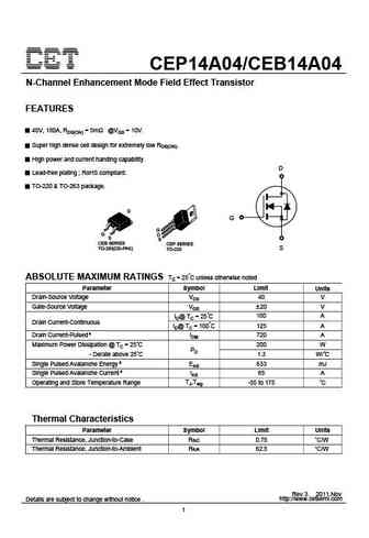
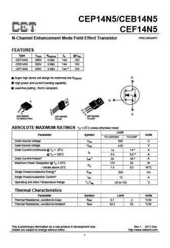
CEP14A04/CEB14A04 N-Channel Enhancement Mode Field Effect Transistor FEATURES 40V, 180A, RDS(ON) = 5m @VGS = 10V. Super high dense cell design for extremely low RDS(ON). High power and current handing capability. D Lead-free plating ; RoHS compliant. TO-220 & TO-263 package. G CEB SERIES CEP SERIES TO-263(DD-PAK) S TO-220 ABSOLUTE MAXIMUM RATINGS Tc = 25 C unless otherwise note... See More ⇒
cep14g04 ceb14g04.pdf
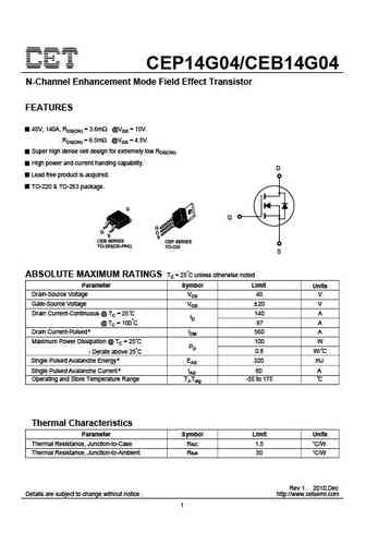
CEP14G04/CEB14G04 N-Channel Enhancement Mode Field Effect Transistor FEATURES 40V, 140A, RDS(ON) = 3.6m @VGS = 10V. RDS(ON) = 6.5m @VGS = 4.5V. Super high dense cell design for extremely low RDS(ON). High power and current handing capability. D Lead free product is acquired. TO-220 & TO-263 package. G CEB SERIES CEP SERIES TO-263(DD-PAK) TO-220 S ABSOLUTE MAXIMUM RATINGS... See More ⇒
cep140n10 ceb140n10.pdf
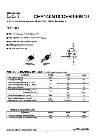
CEP140N10/CEB140N10 N-Channel Enhancement Mode Field Effect Transistor FEATURES 100V, 137A, RDS(ON) = 7.5m @VGS = 10V. Super high dense cell design for extremely low RDS(ON). High power and current handing capability. D Lead-free plating ; RoHS compliant. TO-220 & TO-263 package. G CEB SERIES CEP SERIES TO-263(DD-PAK) S TO-220 ABSOLUTE MAXIMUM RATINGS Tc = 25 C unless otherwise... See More ⇒
cef14p20 cep14p20 ceb14p20.pdf
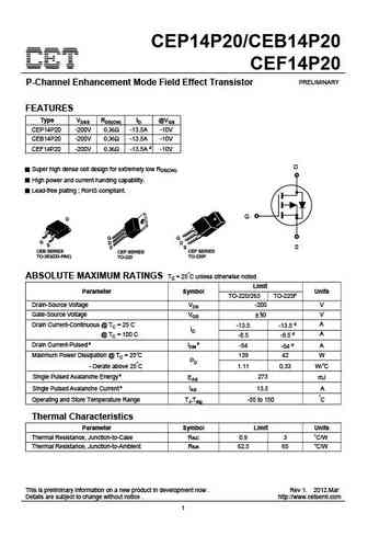
CEP14P20/CEB14P20 CEF14P20 PRELIMINARY P-Channel Enhancement Mode Field Effect Transistor FEATURES Type VDSS RDS(ON) ID @VGS CEP14P20 -200V 0.36 -13.5A -10V CEB14P20 -200V 0.36 -13.5A -10V CEF14P20 -200V 0.36 -13.5A d -10V D Super high dense cell design for extremely low RDS(ON). High power and current handing capability. Lead-free plating ; RoHS compliant. G S CEB SERIE... See More ⇒
Detailed specifications: CEP08N8, CEB20A03, CEP20A03, CEB14G04, CEP14G04, CEB15A03, CEP15A03, CEB14A04, IRF1407, CEB140N10, CEP140N10, CEB16N10L, CEP16N10L, CEB16N10, CEP16N10, CEB13N10L, CEP13N10L
Keywords - CEP14A04 MOSFET specs
CEP14A04 cross reference
CEP14A04 equivalent finder
CEP14A04 pdf lookup
CEP14A04 substitution
CEP14A04 replacement
Need a MOSFET replacement? Our guide shows you how to find a perfect substitute by comparing key parameters and specs
History: 2SK3608-01SJ
🌐 : EN ES РУ

LIST
Last Update
MOSFET: RM50P30DF | CRTT095N12N | CRSS028N10N | CRST030N10N | CRJQ80N65F | ASDM20N20KQ | ASDM20N100Q | ASDM12N65F | ASDM100R750PKQ | ASDM100R160NKQ
Popular searches
2sc945 datasheet | a92 transistor | rfp50n06 | bd140 datasheet | tip2955 | tip35 | 2sk117 | irf9540n datasheet