FDC6308P Datasheet. Specs and Replacement
Type Designator: FDC6308P 📄📄
Type of Transistor: MOSFET
Type of Control Channel: P-Channel
Absolute Maximum Ratings
Pd ⓘ - Maximum Power Dissipation: 0.96 W
|Vds|ⓘ - Maximum Drain-Source Voltage: 20 V
|Vgs|ⓘ - Maximum Gate-Source Voltage: 12 V
|Id| ⓘ - Maximum Drain Current: 1.7 A
Tj ⓘ - Maximum Junction Temperature: 150 °C
Electrical Characteristics
tr ⓘ - Rise Time: 9 nS
Cossⓘ - Output Capacitance: 80 pF
RDSonⓘ - Maximum Drain-Source On-State Resistance: 0.18 Ohm
Package: SUPERSOT6
📄📄 Copy
FDC6308P substitution
- MOSFET ⓘ Cross-Reference Search
FDC6308P datasheet
fdc6308p.pdf
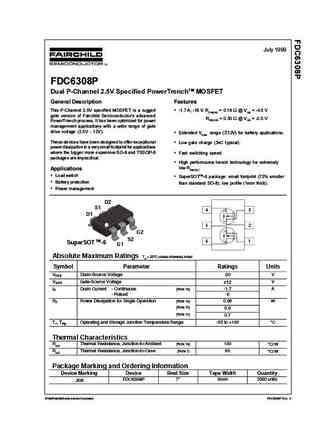
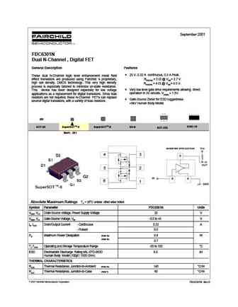
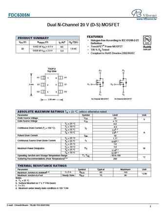
July 1999 FDC6308P Dual P-Channel 2.5V Specified PowerTrenchTM MOSFET General Description Features This P-Channel 2.5V specified MOSFET is a rugged -1.7 A, -18 V. RDS(ON) = 0.18 @ VGS = -4.5 V gate version of Fairchild Semiconductor's advanced RDS(ON) = 0.30 @ VGS = -2.5 V PowerTrench process. It has been optimized for power management applications with a wide range of gate ... See More ⇒
fdc6305n.pdf
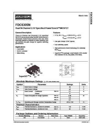
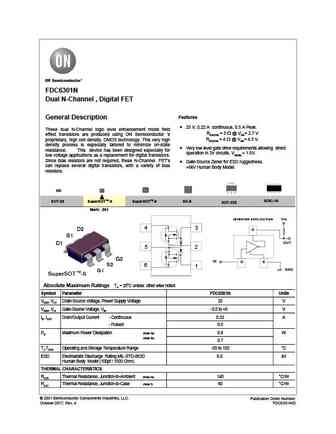
March 1999 FDC6305N Dual N-Channel 2.5V Specified PowerTrenchTM MOSFET General Description Features 2.7 A, 20 V. RDS(ON) = 0.08 @ VGS = 4.5 V These N-Channel low threshold 2.5V specified MOSFETs are produced using Fairchild Semiconductor's RDS(ON) = 0.12 @ VGS = 2.5 V advanced PowerTrench process that has been especially tailored to minimize on-state resistance and Low... See More ⇒
fdc6306p.pdf
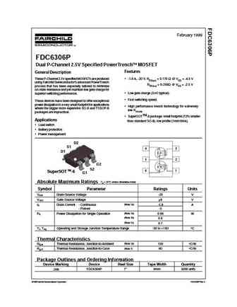
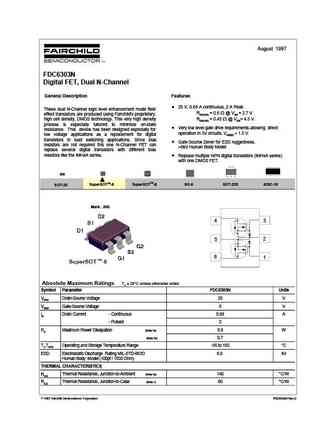
February 1999 FDC6306P Dual P-Channel 2.5V Specified PowerTrench MOSFET Features General Description These P-Channel 2.5V specified MOSFETs are produced -1.9 A, -20 V. RDS(on) = 0.170 @ VGS = -4.5 V using Fairchild Semiconductor's advanced PowerTrench RDS(on) = 0.250 @ VGS = -2.5 V process that has been especially tailored to minimize on-state resistance and yet maintain... See More ⇒
fdc6304p.pdf
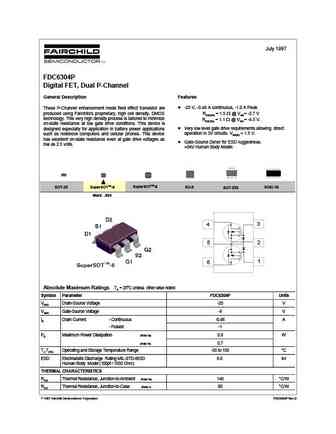
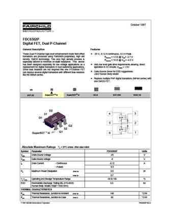
July 1997 FDC6304P Digital FET, Dual P-Channel General Description Features -25 V, -0.46 A continuous, -1.0 A Peak. These P-Channel enhancement mode field effect transistor are produced using Fairchild's proprietary, high cell density, DMOS RDS(ON) = 1.5 @ VGS= -2.7 V technology. This very high density process is tailored to minimize RDS(ON) = 1.1 @ VGS = -4.5 V. on-state ... See More ⇒


Detailed specifications: AS3401, FDC5612, FDC6301N, FDC6302P, FDC6303N, FDC6304P, FDC6305N, FDC6306P, NCEP15T14, FDC633N, FDC634P, FDC636P, FDC637AN, FDC638P, FDC640P, FDC6506P, FDC653N
Keywords - FDC6308P MOSFET specs
FDC6308P cross reference
FDC6308P equivalent finder
FDC6308P pdf lookup
FDC6308P substitution
FDC6308P replacement
Learn how to find the right MOSFET substitute. A guide to cross-reference, check specs and replace MOSFETs in your circuits.
History: FDC638P | HSS2300A | IRFB3607 | HSP80P10 | FDC6303N
🌐 : EN ES РУ

LIST
Last Update
MOSFET: BLM3404 | BL4N90 | SI2309S | SI2301F | BMSN3139 | BMS2302 | BMS2301 | BMDFN2302 | BMDFN2301 | BM8205
Popular searches
2sc373 | a1023 datasheet | 2sc1080 | 2sb618 | 2sc1328 | 2sc1845 transistor | a933 transistor datasheet | a1633 transistor