CED12N10 Specs and Replacement
Type Designator: CED12N10
Type of Transistor: MOSFET
Type of Control Channel: N-Channel
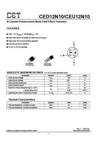
Absolute Maximum Ratings
Pd ⓘ - Maximum Power Dissipation: 43 W
|Vds|ⓘ - Maximum Drain-Source Voltage: 100 V
|Vgs|ⓘ - Maximum Gate-Source Voltage: 20 V
|Id| ⓘ - Maximum Drain Current: 11 A
Tj ⓘ - Maximum Junction Temperature: 175 °C
Electrical Characteristics
tr ⓘ - Rise Time: 7 nS
Cossⓘ - Output Capacitance: 90 pF
RDSonⓘ - Maximum Drain-Source On-State Resistance: 0.18 Ohm
Package: TO251
CED12N10 substitution
- MOSFET ⓘ Cross-Reference Search
CED12N10 datasheet
ceu12n10 ced12n10.pdf

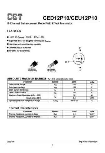
CED12N10/CEU12N10 N-Channel Enhancement Mode Field Effect Transistor FEATURES 100V, 11A, RDS(ON) = 180m @VGS = 10V. Super high dense cell design for extremely low RDS(ON). High power and current handing capability. D Lead free product is acquired. TO-251 & TO-252 package. G D G S CEU SERIES CED SERIES S TO-252(D-PAK) TO-251(I-PAK) ABSOLUTE MAXIMUM RATINGS Tc = 25 C unless o... See More ⇒
ced12n10 ceu12n10.pdf
CED12N10/CEU12N10 N-Channel Enhancement Mode Field Effect Transistor FEATURES 100V, 11A, RDS(ON) = 180m @VGS = 10V. Super high dense cell design for extremely low RDS(ON). High power and current handing capability. D Lead free product is acquired. TO-251 & TO-252 package. G D G S CEU SERIES CED SERIES S TO-252(D-PAK) TO-251(I-PAK) ABSOLUTE MAXIMUM RATINGS Tc = 25 C unless o... See More ⇒
ced12n10.pdf
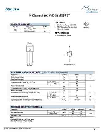
CED12N10 www.VBsemi.tw N-Channel 100 V (D-S) MOSFET FEATURES PRODUCT SUMMARY DT-Trench Power MOSFET VDS (V) RDS(on) ( )ID (A) 175 C Junction Temperature 0.115 at VGS = 10 V 15 100 % Rg Tested 100 0.120 at VGS = 6 V 15 APPLICATIONS Primary Side Switch TO-251 D G S G D S N-Channel MOSFET Top View ABSOLUTE MAXIMUM RATINGS (TC = 25 C, unless otherwise... See More ⇒
ceu12n10l ced12n10l.pdf
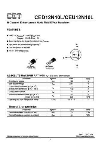
CED12N10L/CEU12N10L N-Channel Enhancement Mode Field Effect Transistor FEATURES 100V, 11A, RDS(ON) = 175m @VGS = 10V. RDS(ON) = 185m @VGS = 5V. Super high dense cell design for extremely low RDS(ON). High power and current handing capability. D Lead free product is acquired. TO-251 & TO-252 package. G D G S CEU SERIES CED SERIES S TO-252(D-PAK) TO-251(I-PAK) ABSOLUTE MA... See More ⇒
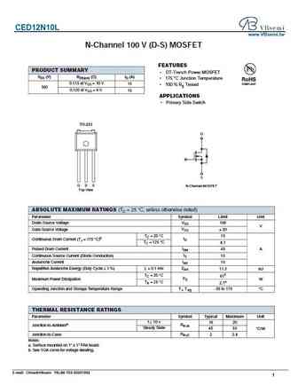
Detailed specifications: CED03N8, CED04N6, CED04N65, CED04N7G, CED05N65, CED06N7, CED07N65A, CED08N6A, 10N60, CED12N10L, CED14G04, CEFF634, CEFF640, CEPF634, CEPF640, CEU01N65, CEU01N65A
Keywords - CED12N10 MOSFET specs
CED12N10 cross reference
CED12N10 equivalent finder
CED12N10 pdf lookup
CED12N10 substitution
CED12N10 replacement
Step-by-step guide to finding a MOSFET replacement. Cross-reference parts and ensure compatibility for your repair or project.
History: CEP10N4
🌐 : EN ES РУ

LIST
Last Update
MOSFET: AKF30N5P0SX | AKF30N10S | AKF20P45D | CM4407 | CM3407 | CM3400 | SVF11N65F | SVF11N65T | FKBB3105 | EHBA036R1
Popular searches
2sc3264 | mp38a | bc546 transistor | bd243 | 2sk170 datasheet | 2n7000 equivalent | tip31 | tip122 transistor