CEP10N65 Specs and Replacement
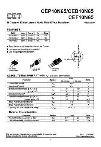
Type Designator: CEP10N65
Type of Transistor: MOSFET
Type of Control Channel: N-Channel
Absolute Maximum Ratings
Pd ⓘ - Maximum Power Dissipation: 200 W
|Vds|ⓘ - Maximum Drain-Source Voltage: 650 V
|Vgs|ⓘ - Maximum Gate-Source Voltage: 30 V
|Id| ⓘ - Maximum Drain Current: 10 A
Tj ⓘ - Maximum Junction Temperature: 175 °C
Electrical Characteristics
tr ⓘ - Rise Time: 73 nS
Cossⓘ - Output Capacitance: 185 pF
Rds ⓘ - Maximum Drain-Source On-State Resistance: 0.85 Ohm
Package: TO220
CEP10N65 substitution
- MOSFET ⓘ Cross-Reference Search
CEP10N65 datasheet
cep10n65 ceb10n65 cef10n65.pdf
CEP10N65/CEB10N65 CEF10N65 N-Channel Enhancement Mode Field Effect Transistor PRELIMINARY FEATURES Type VDSS RDS(ON) ID @VGS CEP10N65 650V 0.85 10A 10V CEB10N65 650V 0.85 10A 10V CEF10N65 650V 0.85 10A d 10V D Super high dense cell design for extremely low RDS(ON). High power and current handing capability. Lead-free plating ; RoHS compliant. G S CEB SERIES CEP SERIES CE... See More ⇒
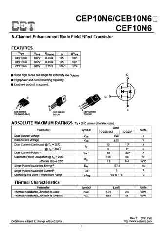
cep10n6 ceb10n6 cef10n6.pdf
CEP10N6/CEB10N6 CEF10N6 N-Channel Enhancement Mode Field Effect Transistor FEATURES Type VDSS RDS(ON) ID @VGS CEP10N6 600V 0.75 10A 10V CEB10N6 600V 0.75 10A 10V CEF10N6 600V 0.75 10A d 10V D Super high dense cell design for extremely low RDS(ON). High power and current handing capability. Lead free product is acquired. G S CEB SERIES CEP SERIES CEF SERIES TO-263(DD-PA... See More ⇒
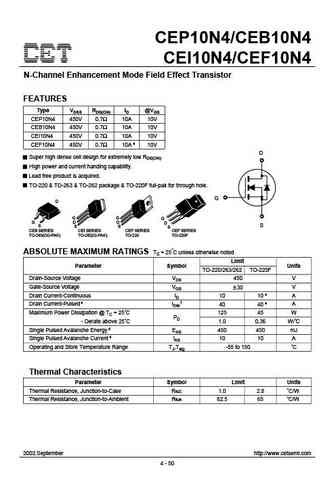
cep10n4 ceb10n4 cei10n4 cef10n4.pdf
CEP10N4/CEB10N4 CEI10N4/CEF10N4 N-Channel Enhancement Mode Field Effect Transistor FEATURES Type VDSS RDS(ON) ID @VGS CEP10N4 450V 0.7 10A 10V CEB10N4 450V 0.7 10A 10V CEI10N4 450V 0.7 10A 10V CEF10N4 450V 0.7 10A e 10V D Super high dense cell design for extremely low RDS(ON). High power and current handing capability. Lead free product is acquired. TO-220 & TO-263 & TO... See More ⇒
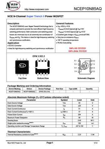
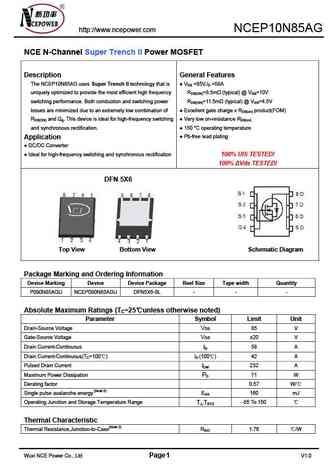
ncep10n85aq.pdf
http //www.ncepower.com NCEP10N85AQ NCE N-Channel Super Trench II Power MOSFET Description General Features The NCEP10N85AQ uses Super Trench II technology that is VDS =85V,ID =51A uniquely optimized to provide the most efficient high frequency RDS(ON)=9.5m (typical) @ VGS=10V switching performance. Both conduction and switching power RDS(ON)=12.5m (typical) @ VGS=4.5V loss... See More ⇒
Detailed specifications: CEF05N6 , CEF10N65 , CEF12N65 , CEH8205 , CEM2539 , CEM73A3G , CEZ3R03 , CEM7808 , IRF1407 , CEP12N65 , CES2336 , CEM3128 , CEM3138 , CEM3172 , CEM3178 , CEM3252 , CEM3252L .
Keywords - CEP10N65 MOSFET specs
CEP10N65 cross reference
CEP10N65 equivalent finder
CEP10N65 pdf lookup
CEP10N65 substitution
CEP10N65 replacement
Need a MOSFET replacement? Our guide shows you how to find a perfect substitute by comparing key parameters and specs


LIST
Last Update
MOSFET: AOT66613L | AOSP21313C | AOSP21311C | AOB66918L | AO3415C | AOTF20N40L | AOTF11N60L | AOT11N60L | AONS21303C | AOI280A60
Popular searches
2sc1213 | a1491 transistor | 2sc897 | 2sa818 | 2sa763 | a933 | 2sa818 replacement | irfb3607 datasheet
