FDG6301N Datasheet. Specs and Replacement
Type Designator: FDG6301N 📄📄
Type of Transistor: MOSFET
Type of Control Channel: N-Channel
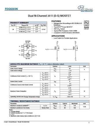
Absolute Maximum Ratings
Pd ⓘ - Maximum Power Dissipation: 0.3 W
|Vds|ⓘ - Maximum Drain-Source Voltage: 25 V
|Vgs|ⓘ - Maximum Gate-Source Voltage: 8 V
|Id| ⓘ - Maximum Drain Current: 0.22 A
Tj ⓘ - Maximum Junction Temperature: 150 °C
Electrical Characteristics
tr ⓘ - Rise Time: 4.5 nS
Cossⓘ - Output Capacitance: 6 pF
RDSonⓘ - Maximum Drain-Source On-State Resistance: 4 Ohm
Package: SC70-6
📄📄 Copy
FDG6301N substitution
- MOSFET ⓘ Cross-Reference Search
FDG6301N datasheet
fdg6301n f085.pdf
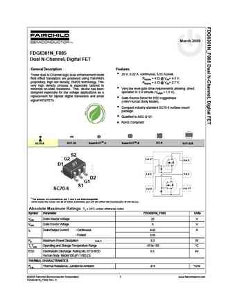
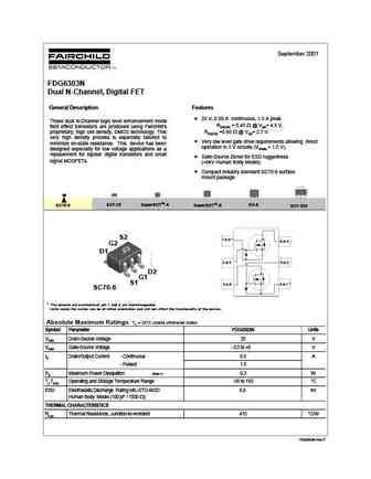
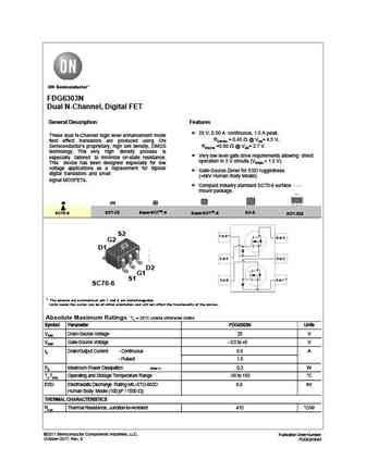
March 2009 FDG6301N_F085 Dual N-Channel, Digital FET General Description Features 25 V, 0.22 A continuous, 0.65 A peak. These dual N-Channel logic level enhancement mode field effect transistors are produced using Fairchild's RDS(ON) = 4 @ VGS= 4.5 V, proprietary, high cell density, DMOS technology. This RDS(ON) = 5 @ VGS= 2.7 V. very high density process is especially tailor... See More ⇒
fdg6301n.pdf
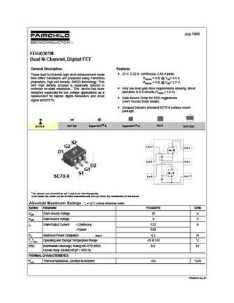
July 1999 FDG6301N Dual N-Channel, Digital FET General Description Features 25 V, 0.22 A continuous, 0.65 A peak. These dual N-Channel logic level enhancement mode field effect transistors are produced using Fairchild's RDS(ON) = 4 @ VGS= 4.5 V, proprietary, high cell density, DMOS technology. This RDS(ON) = 5 @ VGS= 2.7 V. very high density process is especially tailored to ... See More ⇒
fdg6301n.pdf
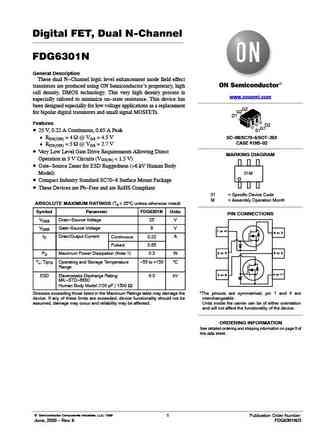
Digital FET, Dual N-Channel FDG6301N General Description These dual N-Channel logic level enhancement mode field effect transistors are produced using ON Semiconductor s proprietary, high cell density, DMOS technology. This very high density process is www.onsemi.com especially tailored to minimize on-state resistance. This device has been designed especially for low voltage applicati... See More ⇒
fdg6301n.pdf
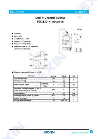
SMD Type MOSFET Dual N-Channel MOSFET FDG6301N (KDG6301N) Features VDS (V) = 25V ID = 220m A (VGS = 4.5V) RDS(ON) 4 (VGS = 4.5V) RDS(ON) 5 (VGS = 2.7V) Gate-Source Zener for ESD ruggedness 1 S 1 S1 4 S2 (>6kV Human Body Model). 2 G1 2 G1 5 G2 3 D2 3 D2 6 D1 1 or 4 6 or 3 2 or 5 5 or 2 4 or 1 3 or 6 Absolute Maximum Ratings T... See More ⇒

Detailed specifications: FDD6690A, AS3402, FDG311N, FDG312P, FDG313N, FDG314P, FDG315N, FDG316P, IRL3713, FDG6302P, FDG6303N, FDG6304P, FDN335N, FDN336P, FDN337N, FDN338P, FDN339AN
Keywords - FDG6301N MOSFET specs
FDG6301N cross reference
FDG6301N equivalent finder
FDG6301N pdf lookup
FDG6301N substitution
FDG6301N replacement
Need a MOSFET replacement? Our guide shows you how to find a perfect substitute by comparing key parameters and specs
MOSFET Parameters. How They Affect Each Other
🌐 : EN ES РУ

LIST
Last Update
MOSFET: MSQ60P04D | MSQ40P07D | MSQ30P40D | MSQ30P15 | MSQ30P07D | MSQ100N03D | MSHM60P14 | MSHM40N085 | MSHM30N46 | MSH60N35D
Popular searches
кт817г характеристики | 2sc1972 | 2n5088 transistor equivalent | 2n5884 | bc640 | 2sc756 | oc44 transistor datasheet | 2sa1210