2N6659 Spec and Replacement
Type Designator: 2N6659
Type of Transistor: MOSFET
Type of Control Channel: N
-Channel
Pd ⓘ
- Maximum Power Dissipation: 6.25
W
|Vds|ⓘ - Maximum Drain-Source Voltage: 35
V
|Vgs|ⓘ - Maximum Gate-Source Voltage: 30
V
|Id| ⓘ - Maximum Drain Current: 2
A
Tj ⓘ - Maximum Junction Temperature: 150
°C
ton ⓘ - Turn-on Time: 8
nS
Cossⓘ -
Output Capacitance: 50
pF
Rds ⓘ - Maximum Drain-Source On-State Resistance: 1.8
Ohm
Package:
TO39
2N6659 Transistor Equivalent Substitute - MOSFET Cross-Reference Search
2N6659 Specs
..1. Size:18K semelab
2n6659.pdf 
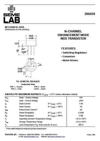
2N6659 MECHANICAL DATA Dimensions in mm (inches) N CHANNEL 8.89 (0.35) ENHANCEMENT MODE 9.40 (0.37) 7.75 (0.305) 8.51 (0.335) MOS TRANSISTOR 4.19 (0.165) 4.95 (0.195) 0.89 max. FEATURES (0.035) 12.70 (0.500) 7.75 (0.305) min. 8.51 (0.335) Switching Regulators dia. Converters 5.08 (0.200) typ. Motor Drivers 2.54 2 (0.100) 1 3 0.66 (0.026) 1.14 (0.045... See More ⇒
0.1. Size:89K vishay
2n6659-2.pdf 
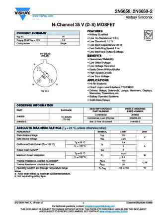
2N6659, 2N6659-2 www.vishay.com Vishay Siliconix N-Channel 35 V (D-S) MOSFET FEATURES PRODUCT SUMMARY Military Qualified VDS (V) 35 Low On-Resistence 1.3 RDS(on) ( ) at VGS = 10 V 1.8 Low Threshold 1.7 V Configuration Single Low Input Capacitance 35 pF Fast Switching Speed 8 ns Low Input and Output Leakage TO-205AD BENEFITS (TO-39) Guarant... See More ⇒
0.2. Size:71K semelab
2n6659x.pdf 
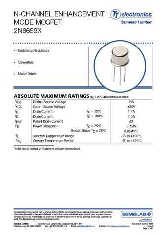
N-CHANNEL ENHANCEMENT MODE MOSFET 2N6659X Switching Regulators Converters Motor Drives ABSOLUTE MAXIMUM RATINGS (TC = 25 C unless otherwise stated) VDS Drain Source Voltage 35V VGS Gate Source Voltage 20V ID TC = 25 C Drain Current 1.4A ID TC = 100 C Drain Current 1.0A IDM1 Pulsed Drain Current 3A PD TC = 25 C Power Dissipation 6.25W... See More ⇒
9.3. Size:11K semelab
2n6653.pdf 
2N6653 Dimensions in mm (inches). Bipolar NPN Device in a Hermetically sealed TO3 25.15 (0.99) 6.35 (0.25) 26.67 (1.05) 9.15 (0.36) Metal Package. 10.67 (0.42) 11.18 (0.44) 1.52 (0.06) 3.43 (0.135) 1 2 Bipolar NPN Device. 3 VCEO = 300V (case) 3.84 (0.151) 4.09 (0.161) 7.92 (0.312) IC = 20A 12.70 (0.50) All Semelab hermetically sealed products can be processed in ... See More ⇒
9.4. Size:12K semelab
2n6654.pdf 
2N6654 Dimensions in mm (inches). Bipolar NPN Device in a Hermetically sealed TO3 25.15 (0.99) 6.35 (0.25) 26.67 (1.05) 9.15 (0.36) Metal Package. 10.67 (0.42) 11.18 (0.44) 1.52 (0.06) 3.43 (0.135) 1 2 Bipolar NPN Device. 3 VCEO = 350V (case) 3.84 (0.151) 4.09 (0.161) 7.92 (0.312) IC = 20A 12.70 (0.50) All Semelab hermetically sealed products can be processed in ... See More ⇒
9.5. Size:11K semelab
2n6655.pdf 
2N6655 Dimensions in mm (inches). Bipolar NPN Device in a Hermetically sealed TO3 25.15 (0.99) 6.35 (0.25) 26.67 (1.05) 9.15 (0.36) Metal Package. 10.67 (0.42) 11.18 (0.44) 1.52 (0.06) 3.43 (0.135) 1 2 Bipolar NPN Device. 3 VCEO = 400V (case) 3.84 (0.151) 4.09 (0.161) 7.92 (0.312) IC = 20A 12.70 (0.50) All Semelab hermetically sealed products can be processed in ... See More ⇒
9.6. Size:147K jmnic
2n6653.pdf 
JMnic Product Specification Silicon NPN Power Transistors 2N6653 DESCRIPTION With TO-3 package High voltage capability Fast switching speeds Low saturation voltage APPLICATIONS Switcing regulators Inverters Solenoid and relay drivers Deflection circuits PINNING (See Fig.2) PIN DESCRIPTION 1 Base 2 Emitter Fig.1 simplified outline (TO-3) and symbol ... See More ⇒
9.7. Size:147K jmnic
2n6654.pdf 
JMnic Product Specification Silicon NPN Power Transistors 2N6654 DESCRIPTION With TO-3 package High voltage capability Fast switching speeds Low saturation voltage APPLICATIONS Switcing regulators Inverters Solenoid and relay drivers Deflection circuits PINNING (See Fig.2) PIN DESCRIPTION 1 Base 2 Emitter Fig.1 simplified outline (TO-3) and symbol ... See More ⇒
9.8. Size:186K inchange semiconductor
2n6653.pdf 
isc Silicon NPN Power Transistor 2N6653 DESCRIPTION High Voltage Capability High Current Current Capability Low Collector Saturation Voltage- High Switching Speed Minimum Lot-to-Lot variations for robust device performance and reliable operation APPLICATIONS Desinged for use in switching and linear applications in military and power conversion. Absolute maximum ratings(Ta... See More ⇒
9.9. Size:186K inchange semiconductor
2n6654.pdf 
isc Silicon NPN Power Transistor 2N6654 DESCRIPTION High Voltage Capability High Current Current Capability Low Collector Saturation Voltage- High Switching Speed Minimum Lot-to-Lot variations for robust device performance and reliable operation APPLICATIONS Desinged for use in switching and linear applications in military and power conversion. Absolute maximum ratings(Ta... See More ⇒
Detailed specifications: 2N4416
, 2N5045
, 2N5484
, 2N5485
, 2N5486
, 2N6656
, 2N6657
, 2N6658
, IRFB4227
, 2N6659-LCC4
, 2N6659-SM
, 2N6660
, 2N6660JAN
, 2N6660JANTX
, 2N6660JANTXV
, 2N6660-LCC4
, 2N6660-SM
.
Keywords - 2N6659 MOSFET specs
2N6659 cross reference
2N6659 equivalent finder
2N6659 lookup
2N6659 substitution
2N6659 replacement
Need a MOSFET replacement?
Our guide shows you how to find a perfect substitute by comparing key parameters and specs