FDS6614A Specs and Replacement
Type Designator: FDS6614A
Type of Transistor: MOSFET
Type of Control Channel: N-Channel
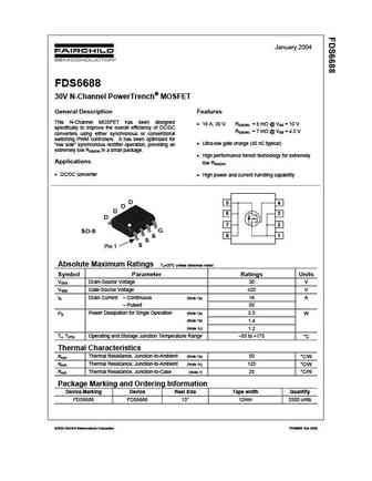
Absolute Maximum Ratings
Pd ⓘ - Maximum Power Dissipation: 2.5 W
|Vds|ⓘ - Maximum Drain-Source Voltage: 30 V
|Vgs|ⓘ - Maximum Gate-Source Voltage: 20 V
|Id| ⓘ - Maximum Drain Current: 9.3 A
Tj ⓘ - Maximum Junction Temperature: 150 °C
Electrical Characteristics
RDSonⓘ - Maximum Drain-Source On-State Resistance: 0.018 Ohm
Package: SO8
FDS6614A substitution
- MOSFET ⓘ Cross-Reference Search
FDS6614A datasheet
fds6614a.pdf
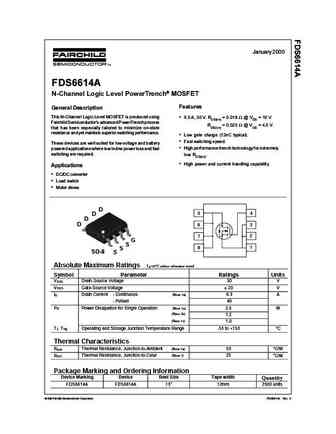
January 2000 FDS6614A N-Channel Logic Level PowerTrench MOSFET Features General Description This N-Channel Logic Level MOSFET is produced using 9.3 A, 30 V. RDS(on) = 0.018 W @ VGS = 10 V Fairchild Semiconductor's advanced PowerTrench process RDS(on) = 0.025 W @ VGS = 4.5 V. that has been especially tailored to minimize on-state resistance and yet maintain superior switching per... See More ⇒
fds6612a.pdf
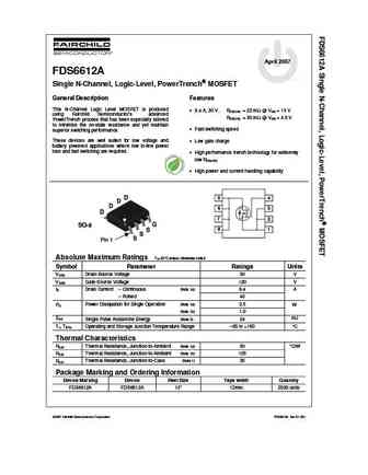
April 2007 FDS6612A tm Single N-Channel, Logic-Level, PowerTrench MOSFET General Description Features This N-Channel Logic Level MOSFET is produced 8.4 A, 30 V. RDS(ON) = 22 m @ VGS = 10 V using Fairchild Semiconductor s advanced RDS(ON) = 30 m @ VGS = 4.5 V PowerTrench process that has been especially tailored to minimize the on-state resistance... See More ⇒
fds6612a.pdf

FDS6612A www.VBsemi.tw N-Channel 20V (D-S) MOSFET FEATURES PRODUCT SUMMARY Halogen-free VDS (V) RDS(on) ( ) ID (A)a Qg (Typ.) TrenchFET Power MOSFET 0.012 at VGS = 10 V 12 20 6.1 nC Optimized for High-Side Synchronous 0.015 at VGS = 4.5 V 11 Rectifier Operation 100 % Rg Tested 100 % UIS Tested APPLICATIONS Notebook CPU Core - High-Side Switch SO... See More ⇒
fds6682.pdf
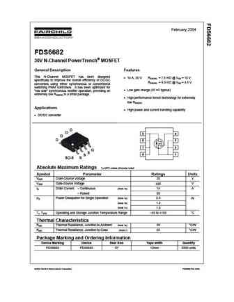
February 2004 FDS6682 30V N-Channel PowerTrench MOSFET General Description Features This N-Channel MOSFET has been designed 14 A, 30 V. RDS(ON) = 7.5 m @ VGS = 10 V specifically to improve the overall efficiency of DC/DC RDS(ON) = 9.0 m @ VGS = 4.5 V converters using either synchronous or conventional switching PWM controllers. It has been optimized for Low gate charge (... See More ⇒
fds6670as.pdf
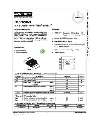
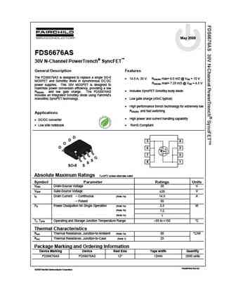
July 2010 FDS6670AS 30V N-Channel PowerTrench SyncFET General Description Features The FDS6670AS is designed to replace a single SO-8 13.5 A, 30 V. RDS(ON) max= 9.0 m @ VGS = 10 V MOSFET and Schottky diode in synchronous DC DC RDS(ON) max= 11.5 m @ VGS = 4.5 V power supplies. This 30V MOSFET is designed to maximize power conversion efficiency, providing a low Inclu... See More ⇒
fds6679.pdf
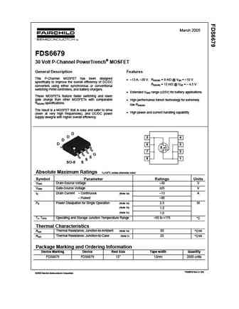
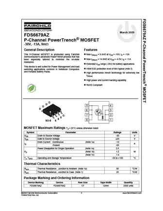
March 2005 FDS6679 30 Volt P-Channel PowerTrench MOSFET General Description Features This P-Channel MOSFET has been designed 13 A, 30 V. RDS(ON) = 9 m @ VGS = 10 V specifically to improve the overall efficiency of DC/DC RDS(ON) = 13 m @ VGS = 4.5 V converters using either synchronous or conventional switching PWM controllers, and battery chargers. ... See More ⇒
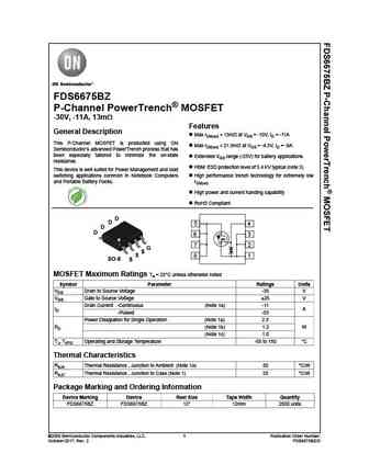
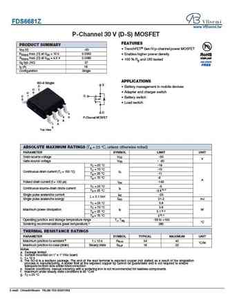
fds6675bz.pdf
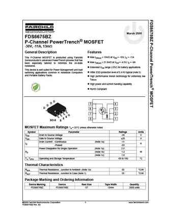
March 2009 FDS6675BZ tm P-Channel PowerTrench MOSFET -30V, -11A, 13m General Description Features Max rDS(on) = 13m at VGS = -10V, ID = -11A This P-Channel MOSFET is producted using Fairchild Semiconductor s advanced PowerTrench process that has Max rDS(on) = 21.8m at VGS = -4.5V, ID = -9A been especially tailored to minimize the on-state resistance. Extended VGS ... See More ⇒
fds6609a.pdf
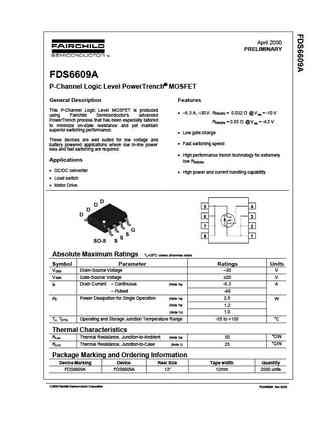
April 2000 PRELIMINARY FDS6609A P-Channel Logic Level PowerTrench MOSFET General Description Features This P-Channel Logic Level MOSFET is produced 6.3 A, 30 V . R = 0.032 @ VGS = -10 V DS(ON) using Fairchild Semiconductor's advanced PowerTrench process that has been especially tailored R = 0.05 @ VGS = -4.5 V DS(ON) to minimize on-state resistance and yet maintain... See More ⇒
fds6699s.pdf
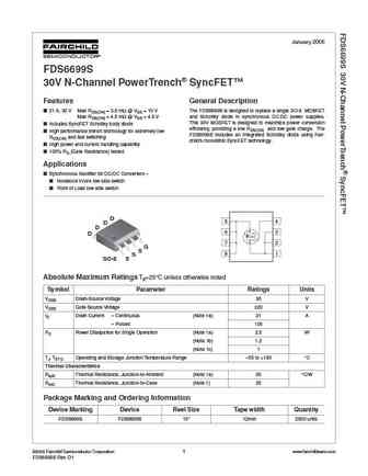
January 2005 FDS6699S 30V N-Channel PowerTrench SyncFET Features General Description 21 A, 30 V Max RDS(ON) = 3.6 m @ VGS = 10 V The FDS6699S is designed to replace a single SO-8 MOSFET Max RDS(ON) = 4.5 m @ VGS = 4.5 V and Schottky diode in synchronous DC DC power supplies. This 30V MOSFET is designed to maximize power conversion Includes SyncFET Schottky body diode ... See More ⇒
fds6675a.pdf
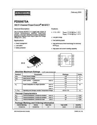
February 2003 FDS6675A 30V P-Channel PowerTrench MOSFET General Description Features This P-Channel MOSFET is a rugged gate version of 11 A, 30 V RDS(ON) = 13 m @ VGS = 10 V Fairchild Semiconductor s advanced PowerTrench RDS(ON) = 19 m @ VGS = 4.5 V process. It has been optimized for power management applications requiring a wide rang... See More ⇒
fds6672a.pdf

April 2001 FDS6672A 30V N-Channel PowerTrench MOSFET General Description Features This N-Channel MOSFET has been designed 12.5 A, 30 V. RDS(ON) = 8 m @ VGS = 10 V specifically to improve the overall efficiency of DC/DC RDS(ON) = 9.5 m @ VGS = 4.5 V converters using either synchronous or conventional switching PWM controllers. It has been optimized f... See More ⇒
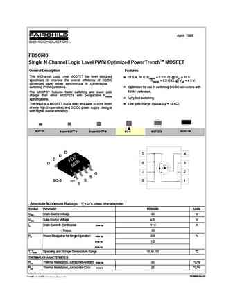
fds6680.pdf

April 1998 FDS6680 Single N-Channel Logic Level PWM Optimized PowerTrenchTM MOSFET General Description Features This N-Channel Logic Level MOSFET has been designed 11.5 A, 30 V. RDS(ON) = 0.010 @ VGS = 10 V specifically to improve the overall efficiency of DC/DC RDS(ON) = 0.015 @ VGS = 4.5 V. converters using either synchronous or conventional switching PWM controllers. O... See More ⇒
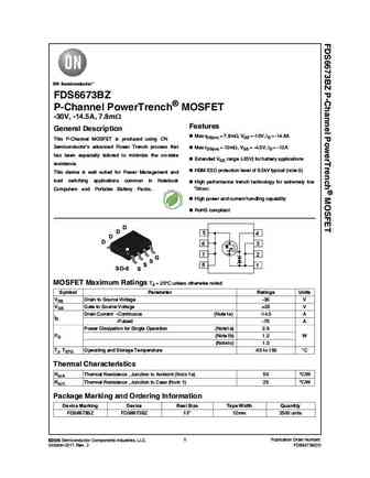
fds6673bz.pdf
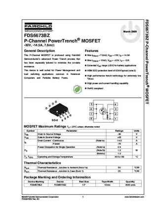
March 2009 FDS6673BZ P-Channel PowerTrench MOSFET -30V, -14.5A, 7.8m General Description Features This P-Channel MOSFET is produced using Fairchild Max rDS(on) = 7.8m , VGS = -10V, ID = -14.5A Semiconductor s advanced Power Trench process that Max rDS(on) = 12m , VGS = -4.5V, ID = -12A has been especially tailored to minimize the on-state Extended VGS range (-25V) for b... See More ⇒
fds6681z.pdf
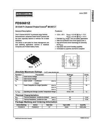
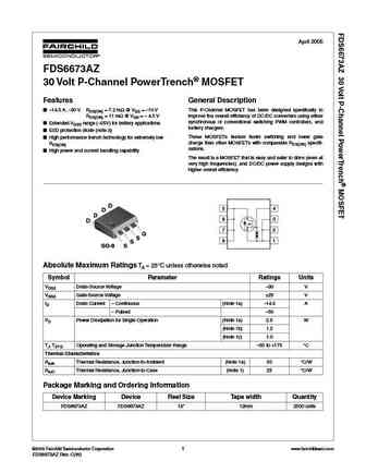
June 2005 FDS6681Z 30 Volt P-Channel PowerTrench MOSFET General Description Features This P-Channel MOSFET is produced using Fairchild 20 A, 30 V. RDS(ON) = 4.6 m @ VGS = 10 V Semiconductor s advanced PowerTrench process that RDS(ON) = 6.5 m @ VGS = 4.5 V has been especially tailored to minimize the on-state Extended VGSS range ( 25V) for battery a... See More ⇒
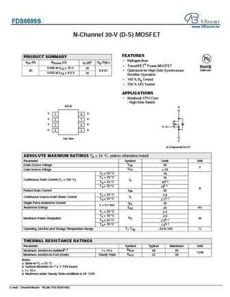
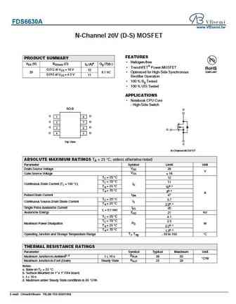
fds6630a.pdf
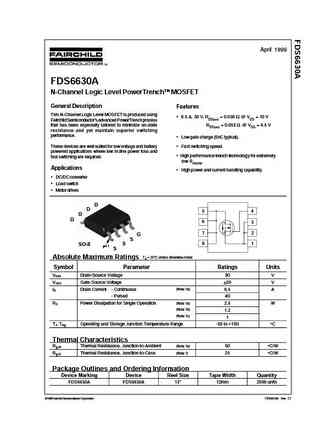
April 1999 FDS6630A N-Channel Logic Level PowerTrenchTM MOSFET General Description Features This N-Channel Logic Level MOSFET is produced using 6.5 A, 30 V. RDS(on) = 0.038 @ VGS = 10 V Fairchild Semiconductor's advanced PowerTrench process that has been especially tailored to minimize on-state RDS(on) = 0.053 @ VGS = 4.5 V resistance and yet maintain superior switching pe... See More ⇒
fds6676as.pdf
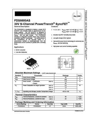
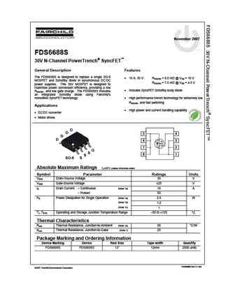
May 2008 tm FDS6676AS 30V N-Channel PowerTrench SyncFET General Description Features The FDS6676AS is designed to replace a single SO-8 14.5 A, 30 V. RDS(ON) max= 6.0 m @ VGS = 10 V MOSFET and Schottky diode in synchronous DC DC RDS(ON) max= 7.25 m @ VGS = 4.5 V power supplies. This 30V MOSFET is designed to maximize power conversion efficiency, providing a low ... See More ⇒
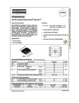
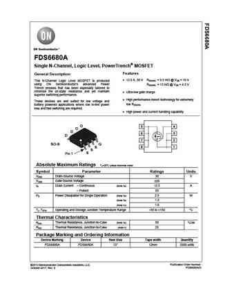
fds6690a.pdf
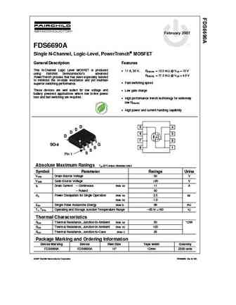
February 2007 tm FDS6690A Single N-Channel, Logic-Level, PowerTrench MOSFET General Description Features This N-Channel Logic Level MOSFET is produced 11 A, 30 V. RDS(ON) = 12.5 m @ VGS = 10 V using Fairchild Semiconductor s advanced RDS(ON) = 17.0 m @ VGS = 4.5 V PowerTrench process that has been especially tailored to minimize the on-state resi... See More ⇒
fds6679z.pdf
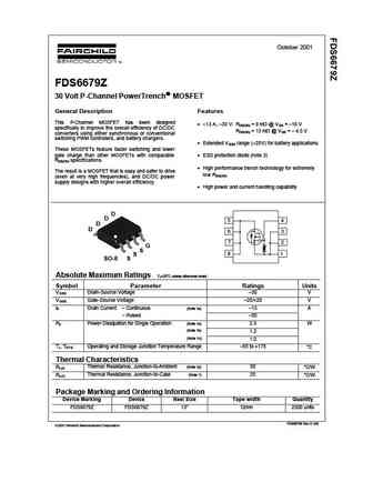
October 2001 FDS6679Z 30 Volt P-Channel PowerTrench MOSFET General Description Features This P-Channel MOSFET has been designed 13 A, 30 V. R = 9 m @ V = 10 V DS(ON) GS specifically to improve the overall efficiency of DC/DC R = 13 m @ V = 4.5 V DS(ON) GS converters using either synchronous or conventional switching PWM controllers, and battery charge... See More ⇒
fds6680a.pdf
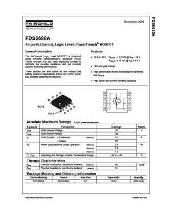
November 2004 FDS6680A Single N-Channel, Logic Level, PowerTrench MOSFET General Description Features This N-Channel Logic Level MOSFET is produced 12.5 A, 30 V RDS(ON) = 9.5 m @ VGS = 10 V using Fairchild Semiconductor s advanced Power RDS(ON) = 13 m @ VGS = 4.5 V Trench process that has been especially tailored to minimize the on-state resistance and yet maint... See More ⇒
fds6679az.pdf
March 2009 FDS6679AZ tm P-Channel PowerTrench MOSFET -30V, -13A, 9m General Description Features This P-Channel MOSFET is producted using Fairchild Max rDS(on) = 9.3m at VGS = -10V, ID = -13A Semiconductor s advanced PowerTrench process that has Max rDS(on) = 14.8m at VGS = -4.5V, ID = -11A been especially tailored to minimize the on-state resistance. Extended VGS r... See More ⇒
fds6690as.pdf
May 2008 tm FDS6690AS 30V N-Channel PowerTrench SyncFET General Description Features The FDS6690AS is designed to replace a single SO-8 10 A, 30 V. RDS(ON) max= 12 m @ VGS = 10 V MOSFET and Schottky diode in synchronous DC DC RDS(ON) max= 15 m @ VGS = 4.5 V power supplies. This 30V MOSFET is designed to maximize power conversion efficiency, providing a low ... See More ⇒
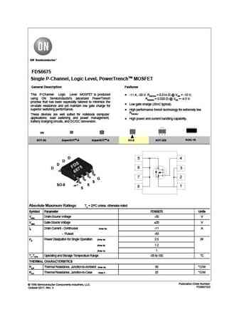
fds6675.pdf
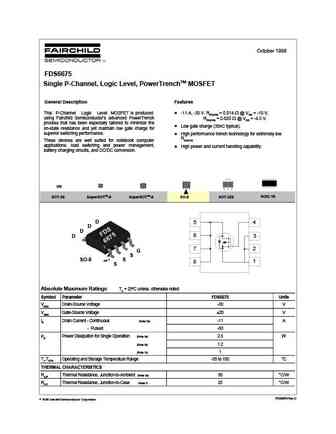
October 1998 FDS6675 Single P-Channel, Logic Level, PowerTrenchTM MOSFET General Description Features This P-Channel Logic Level MOSFET is produced -11 A, -30 V. RDS(ON) = 0.014 @ VGS = -10 V, using Fairchild Semiconductor's advanced PowerTrench RDS(ON) = 0.020 @ VGS = -4.5 V. process that has been especially tailored to minimize the Low gate charge (30nC typical). on-state ... See More ⇒
fds6690.pdf
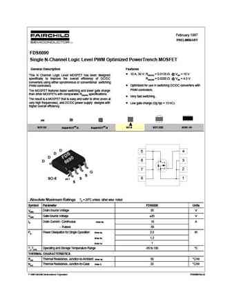
February 1997 PRELIMINARY FDS6690 Single N-Channel Logic Level PWM Optimized PowerTrench MOSFET General Description Features 10 A, 30 V. RDS(ON) = 0.0135 @ VGS = 10 V This N Channel Logic Level MOSFET has been designed specifically to improve the overall efficiency of DC/DC RDS(ON) = 0.0200 @ VGS = 4.5 V. converters using either synchronous or conventional switching Optimize... See More ⇒
fds6688.pdf
January 2004 FDS6688 30V N-Channel PowerTrench MOSFET General Description Features This N-Channel MOSFET has been designed 16 A, 30 V. RDS(ON) = 6 m @ VGS = 10 V specifically to improve the overall efficiency of DC/DC RDS(ON) = 7 m @ VGS = 4.5 V converters using either synchronous or conventional switching PWM controllers. It has been optimized for Ultra-low gate charge... See More ⇒
fds6680s.pdf
April 1998 FDS6680 Single N-Channel Logic Level PWM Optimized PowerTrenchTM MOSFET General Description Features This N-Channel Logic Level MOSFET has been designed 11.5 A, 30 V. RDS(ON) = 0.010 @ VGS = 10 V specifically to improve the overall efficiency of DC/DC RDS(ON) = 0.015 @ VGS = 4.5 V. converters using either synchronous or conventional switching PWM controllers. O... See More ⇒
fds6670a.pdf
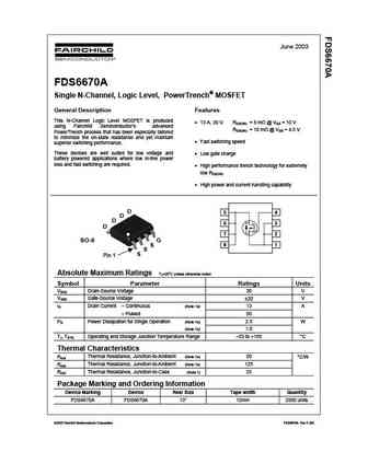
June 2003 FDS6670A Single N-Channel, Logic Level, PowerTrench MOSFET General Description Features This N-Channel Logic Level MOSFET is produced 13 A, 30 V. RDS(ON) = 8 m @ VGS = 10 V using Fairchild Semiconductor s advanced RDS(ON) = 10 m @ VGS = 4.5 V PowerTrench process that has been especially tailored to minimize the on-state resistance and yet maintain Fast switc... See More ⇒
fds6692a.pdf
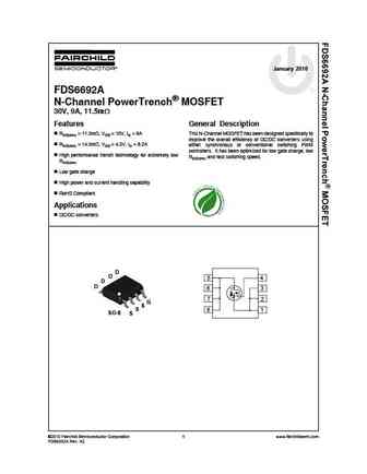
January 2010 FDS6692A N-Channel PowerTrench MOSFET 30V, 9A, 11.5m Features General Description RDS(ON) = 11.5m , VGS = 10V, ID = 9A This N-Channel MOSFET has been designed specifically to improve the overall efficiency of DC/DC converters using RDS(ON) = 14.5m , VGS = 4.5V, ID = 8.2A either synchronous or conventional switching PWM controllers. It has been optimized for ... See More ⇒
fds6680as.pdf
May 2008 tm FDS6680AS 30V N-Channel PowerTrench SyncFET General Description Features The FDS6680AS is designed to replace a single SO-8 11.5 A, 30 V. RDS(ON) max= 10.0 m @ VGS = 10 V MOSFET and Schottky diode in synchronous DC DC RDS(ON) max= 12.5 m @ VGS = 4.5 V power supplies. This 30V MOSFET is designed to maximize power conversion efficiency, providing a low... See More ⇒
fds6673bz f085.pdf
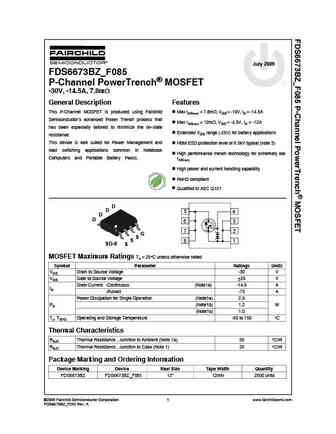
July 2009 FDS6673BZ_F085 P-Channel PowerTrench MOSFET -30V, -14.5A, 7.8m General Description Features This P-Channel MOSFET is produced using Fairchild Max rDS(on) = 7.8m , VGS = -10V, ID = -14.5A Semiconductor s advanced Power Trench process that Max rDS(on) = 12m , VGS = -4.5V, ID = -12A has been especially tailored to minimize the on-state Extended VGS range (-25V) ... See More ⇒
fds6688s.pdf
November 2007 tm FDS6688S 30V N-Channel PowerTrench SyncFET General Description Features The FDS6688S is designed to replace a single SO-8 16 A, 30 V. RDS(ON) = 6.0 m @ VGS = 10 V MOSFET and Schottky diode in synchronous DC DC RDS(ON) = 7.5 m @ VGS = 4.5 V power supplies. This 30V MOSFET is designed to maximize power conversion efficiency, providing a low ... See More ⇒
fds6694.pdf
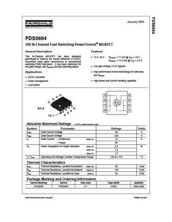
January 2004 FDS6694 30V N-Channel Fast Switching PowerTrench MOSFET General Description Features This N-Channel MOSFET has been designed 12 A, 30 V. RDS(ON) = 11 m @ VGS = 10 V specifically to improve the overall efficiency of DC/DC RDS(ON) = 13.5 m @ VGS = 4.5 V converters using either synchronous or conventional switching PWM controllers. It has been optimized for Lo... See More ⇒
fds6688as.pdf

November 2008 tm FDS6688AS 30V N-Channel PowerTrench SyncFET General Description Features The FDS6688AS is designed to replace a single SO-8 14.5 A, 30 V. RDS(ON) max= 6.0 m @ VGS = 10 V MOSFET and Schottky diode in synchronous DC DC RDS(ON) max= 7.3 m @ VGS = 4.5 V power supplies. This 30V MOSFET is designed to maximize power conversion efficiency, providing a ... See More ⇒
fds6682.pdf

Is Now Part of To learn more about ON Semiconductor, please visit our website at www.onsemi.com Please note As part of the Fairchild Semiconductor integration, some of the Fairchild orderable part numbers will need to change in order to meet ON Semiconductor s system requirements. Since the ON Semiconductor product management systems do not have the ability to manage part nomenclatur... See More ⇒
fds6670as.pdf

Is Now Part of To learn more about ON Semiconductor, please visit our website at www.onsemi.com Please note As part of the Fairchild Semiconductor integration, some of the Fairchild orderable part numbers will need to change in order to meet ON Semiconductor s system requirements. Since the ON Semiconductor product management systems do not have the ability to manage part nomenclatur... See More ⇒
fds6675bz.pdf
FDS6675BZ P-Channel PowerTrench MOSFET -30V, -11A, 13m Features General Description Max rDS(on) = 13m at VGS = -10V, ID = -11A This P-Channel MOSFET is producted using ON Max rDS(on) = 21.8m at VGS = -4.5V, ID = -9A Semiconductor s advanced PowerTrench process that has been especially tailored to minimize the on-state Extended VGS range (-25V) for battery application... See More ⇒
fds6673bz.pdf
FDS6673BZ P-Channel PowerTrench MOSFET -30V, -14.5A, 7.8m Features General Description Max rDS(on) = 7.8m , VGS = -10V, ID = -14.5A This P-Channel MOSFET is produced using ON Semiconductor s advanced Power Trench process that Max rDS(on) = 12m , VGS = -4.5V, ID = -12A has been especially tailored to minimize the on-state Extended VGS range (-25V) for battery applicatio... See More ⇒
fds6680a.pdf
FDS6680A Single N-Channel, Logic Level, PowerTrench MOSFET Features General Description 12.5 A, 30 V RDS(ON) = 9.5 m @ VGS = 10 V This N-Channel Logic Level MOSFET is produced using ON Semiconductor s advanced Power RDS(ON) = 13 m @ VGS = 4.5 V Trench process that has been especially tailored to minimize the on-state resistance and yet maintain Ultra-low gate... See More ⇒
fds6679az.pdf

Is Now Part of To learn more about ON Semiconductor, please visit our website at www.onsemi.com ON Semiconductor and the ON Semiconductor logo are trademarks of Semiconductor Components Industries, LLC dba ON Semiconductor or its subsidiaries in the United States and/or other countries. ON Semiconductor owns the rights to a number of patents, trademarks, copyrights, trade secrets, and oth... See More ⇒
fds6690as.pdf

Is Now Part of To learn more about ON Semiconductor, please visit our website at www.onsemi.com Please note As part of the Fairchild Semiconductor integration, some of the Fairchild orderable part numbers will need to change in order to meet ON Semiconductor s system requirements. Since the ON Semiconductor product management systems do not have the ability to manage part nomenclatur... See More ⇒
fds6675.pdf
FDS6675 Single P-Channel, Logic Level, PowerTrenchTM MOSFET General Description Features This P-Channel Logic Level MOSFET is produced -11 A, -30 V. RDS(ON) = 0.014 @ VGS = -10 V, using ON Semiconductor's advanced PowerTrench RDS(ON) = 0.020 @ VGS = -4.5 V. process that has been especially tailored to minimize the Low gate charge (30nC typical). on-state resistance and yet ... See More ⇒
fds6670a.pdf

Is Now Part of To learn more about ON Semiconductor, please visit our website at www.onsemi.com Please note As part of the Fairchild Semiconductor integration, some of the Fairchild orderable part numbers will need to change in order to meet ON Semiconductor s system requirements. Since the ON Semiconductor product management systems do not have the ability to manage part nomenclatur... See More ⇒
fds6680as.pdf

Is Now Part of To learn more about ON Semiconductor, please visit our website at www.onsemi.com Please note As part of the Fairchild Semiconductor integration, some of the Fairchild orderable part numbers will need to change in order to meet ON Semiconductor s system requirements. Since the ON Semiconductor product management systems do not have the ability to manage part nomenclatur... See More ⇒
fds6670as.pdf

FDS6670AS www.VBsemi.tw N-Channel 20V (D-S) MOSFET FEATURES PRODUCT SUMMARY Halogen-free VDS (V) RDS(on) ( ) ID (A)a Qg (Typ.) TrenchFET Power MOSFET 0.012 at VGS = 10 V 12 20 6.1 nC Optimized for High-Side Synchronous 0.015 at VGS = 4.5 V 11 Rectifier Operation 100 % Rg Tested 100 % UIS Tested APPLICATIONS Notebook CPU Core - High-Side Switch S... See More ⇒
fds6699s.pdf
FDS6699S www.VBsemi.tw N-Channel 30-V (D-S) MOSFET FEATURES PRODUCT SUMMARY Halogen-free VDS (V) RDS(on) ( ) ID (A)a Qg (Typ.) TrenchFET Power MOSFET 0.004 at VGS = 10 V 18 30 6.8 nC Optimized for High-Side Synchronous 0.005 at VGS = 4.5 V 16 Rectifier Operation 100 % Rg Tested 100 % UIS Tested APPLICATIONS Notebook CPU Core - High-Side Switch S... See More ⇒
fds6673bz.pdf

FDS6673BZ www.VBsemi.tw P-Channel 30-V (D-S) MOSFET FEATURES PRODUCT SUMMARY Halogen-free VDS (V) RDS(on) ( ) ID (A)d Qg (Typ.) TrenchFET Power MOSFET 0.011 at VGS = - 10 V - 13.5 100 % Rg Tested RoHS - 30 29.5 nC COMPLIANT 100 % UIS Tested 0.015 at VGS = - 4.5 V - 11.6 APPLICATIONS Load Switch Notebook Adaptor Switch SO-8 S S 1 8 D S D 2 7 G ... See More ⇒
fds6681z.pdf
FDS6681Z www.VBsemi.tw P-Channel 30 V (D-S) MOSFET FEATURES PRODUCT SUMMARY TrenchFET Gen IV p-channel power MOSFET VDS (V) -30 RDS(on) max. ( ) at VGS = 10 V 0.0050 Enables higher power density RDS(on) max. ( ) at VGS = 4.5 V 0.0080 100 % Rg and UIS tested Qg typ. (nC) 27 ID (A) 18 Configuration Single APPLICATIONS SO-8 Single S D Battery management in m... See More ⇒
fds6630a.pdf
FDS6630A www.VBsemi.tw N-Channel 20V (D-S) MOSFET FEATURES PRODUCT SUMMARY Halogen-free VDS (V) RDS(on) ( ) ID (A)a Qg (Typ.) TrenchFET Power MOSFET 0.012 at VGS = 10 V 12 20 6.1 nC Optimized for High-Side Synchronous 0.015 at VGS = 4.5 V 11 Rectifier Operation 100 % Rg Tested 100 % UIS Tested APPLICATIONS Notebook CPU Core - High-Side Switch SO... See More ⇒
fds6675b.pdf
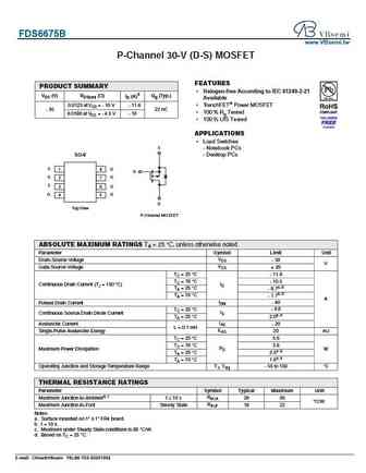
FDS6675B www.VBsemi.tw P-Channel 30-V (D-S) MOSFET FEATURES PRODUCT SUMMARY Halogen-free According to IEC 61249-2-21 VDS (V) RDS(on) ( ) ID (A)d Qg (Typ.) Available 0.0125 at VGS = - 10 V - 11.6 TrenchFET Power MOSFET - 30 22 nC 100 % Rg Tested 0.0180 at VGS = - 4.5 V - 10 100 % UIS Tested APPLICATIONS Load Switches S - Notebook PCs SO-8 - Desktop PCs... See More ⇒
fds6679az.pdf
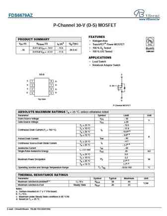
FDS6679AZ www.VBsemi.tw P-Channel 30-V (D-S) MOSFET FEATURES PRODUCT SUMMARY Halogen-free VDS (V) RDS(on) ( ) ID (A)d Qg (Typ.) TrenchFET Power MOSFET 0.011 at VGS = - 10 V - 13.5 100 % Rg Tested RoHS - 30 29.5 nC COMPLIANT 100 % UIS Tested 0.015 at VGS = - 4.5 V - 11.6 APPLICATIONS Load Switch Notebook Adaptor Switch SO-8 S S 1 8 D S D 2 7 G ... See More ⇒
fds6694.pdf
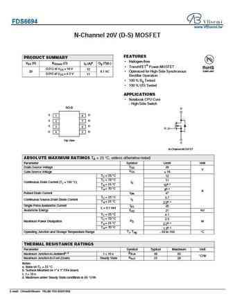
FDS6694 www.VBsemi.tw N-Channel 20V (D-S) MOSFET FEATURES PRODUCT SUMMARY Halogen-free VDS (V) RDS(on) ( ) ID (A)a Qg (Typ.) TrenchFET Power MOSFET 0.012 at VGS = 10 V 12 20 6.1 nC Optimized for High-Side Synchronous 0.015 at VGS = 4.5 V 11 Rectifier Operation 100 % Rg Tested 100 % UIS Tested APPLICATIONS Notebook CPU Core - High-Side Switch SO-... See More ⇒
Detailed specifications: FDS4953, FDS5680, FDS5690, FDS6375, FDS6570A, FDS6575, FDS6576, FDS6612A, 2N7002, FDS6630A, FDS6670A, FDS6675, FDS6680, FDS6680A, FDS6685, FDS6690A, FDS6875
Keywords - FDS6614A MOSFET specs
FDS6614A cross reference
FDS6614A equivalent finder
FDS6614A pdf lookup
FDS6614A substitution
FDS6614A replacement
Learn how to find the right MOSFET substitute. A guide to cross-reference, check specs and replace MOSFETs in your circuits.
🌐 : EN ES РУ

LIST
Last Update
MOSFET: AUW033N08BG | AUW025N10 | AUR030N10 | AUR020N10 | AUR020N085 | AUR014N10 | AUP074N10 | AUP065N10 | AUP062N08BG | AUP060N08AG
Popular searches
mosfet k8a50d | sl100 transistor | d2499 datasheet | 6r190p6 datasheet | 2n270 | 2n2924 | mpsa65 | 2sa794