IRF623FI Specs and Replacement
Type Designator: IRF623FI
Type of Transistor: MOSFET
Type of Control Channel: N-Channel
Absolute Maximum Ratings
Pd ⓘ - Maximum Power Dissipation: 30 W
|Vds|ⓘ - Maximum Drain-Source Voltage: 150 V
|Vgs|ⓘ - Maximum Gate-Source Voltage: 20 V
|Id| ⓘ - Maximum Drain Current: 3.5 A
Tj ⓘ - Maximum Junction Temperature: 150 °C
Electrical Characteristics
tr ⓘ - Rise Time: 60 nS
Cossⓘ - Output Capacitance: 300 pF
RDSonⓘ - Maximum Drain-Source On-State Resistance: 1.2 Ohm
Package: ISOWATT220
IRF623FI substitution
- MOSFET ⓘ Cross-Reference Search
IRF623FI datasheet
irfs624b irf624b.pdf
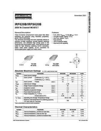
November 2001 IRF624B/IRFS624B 250V N-Channel MOSFET General Description Features These N-Channel enhancement mode power field effect 4.1A, 250V, RDS(on) = 1.1 @VGS = 10 V transistors are produced using Fairchild s proprietary, Low gate charge ( typical 13.5 nC) planar, DMOS technology. Low Crss ( typical 9.5 pF) This advanced technology has been especially tailored to ... See More ⇒
irf6216pbf.pdf
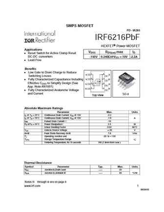
SMPS MOSFET PD - 95293 IRF6216PbF HEXFET Power MOSFET Applications VDSS RDS(on) max ID l Reset Switch for Active Clamp Reset DC-DC converters -150V 0.240W@VGS =-10V -2.2A l Lead-Free Benefits l Low Gate to Drain Charge to Reduce A 1 8 S D Switching Losses 2 7 S D l Fully Characterized Capacitance Including 3 Effective COSS to Simplify Design (See 6 S D App. Note AN1001) 4... See More ⇒
irf6218spbf.pdf
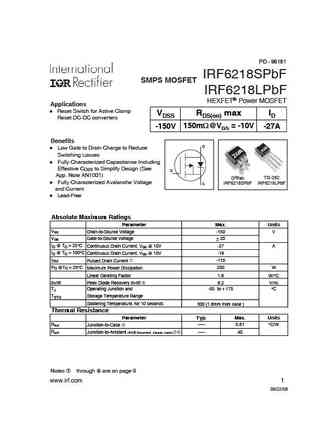
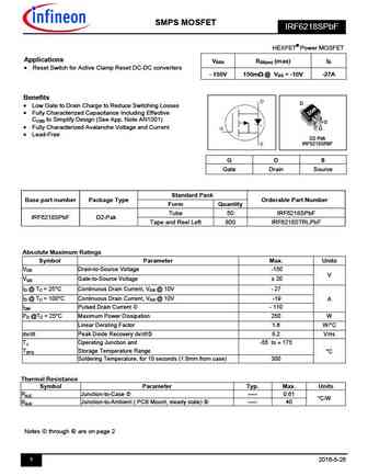
PD - 96181 IRF6218SPbF SMPS MOSFET IRF6218LPbF HEXFET Power MOSFET Applications l Reset Switch for Active Clamp VDSS RDS(on) max ID Reset DC-DC converters 150m @VGS = -10V -27A -150V Benefits D l Low Gate to Drain Charge to Reduce Switching Losses l Fully Characterized Capacitance Including Effective COSS to Simplify Design (See G App. Note AN1001) D2Pak TO-262 l Fully Cha... See More ⇒
irf6215s.pdf
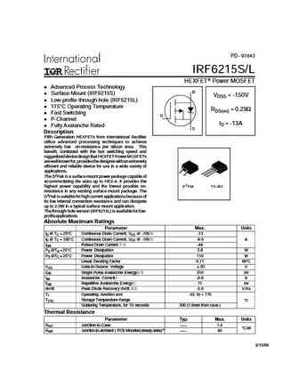
PD - 91643 IRF6215S/L HEXFET Power MOSFET Advanced Process Technology D Surface Mount (IRF6215S) VDSS = -150V Low-profile through-hole (IRF6215L) 175 C Operating Temperature RDS(on) = 0.29 Fast Switching G P-Channel ID = -13A Fully Avalanche Rated S Description Fifth Generation HEXFETs from International Rectifier utilize advanced processing techniques to achieve ... See More ⇒
auirf6215.pdf
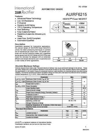
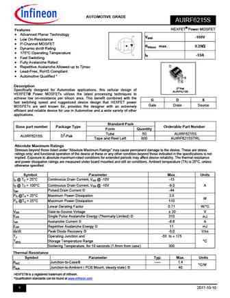
PD - 97564 AUTOMOTIVE GRADE AUIRF6215 Features l Advanced Planar Technology HEXFET Power MOSFET l Low On-Resistance l P-Channel D V(BR)DSS -150V l Dynamic dv/dt Rating RDS(on) max. 0.29 l 175 C Operating Temperature G l Fast Switching ID -13A S l Fully Avalanche Rated l Repetitive Avalanche Allowed up to Tjmax l Lead-Free, RoHS Compliant l Automotive Qualified D D... See More ⇒
irf6218l.pdf
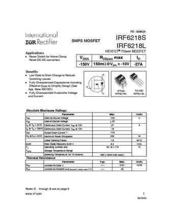
PD - 95863A IRF6218S SMPS MOSFET IRF6218L HEXFET Power MOSFET Applications l Reset Switch for Active Clamp VDSS RDS(on) max ID Reset DC-DC converters 150m @VGS = -10V -27A -150V Benefits D l Low Gate to Drain Charge to Reduce Switching Losses l Fully Characterized Capacitance Including Effective COSS to Simplify Design (See G App. Note AN1001) TO-262 D2Pak l Fully Charact... See More ⇒
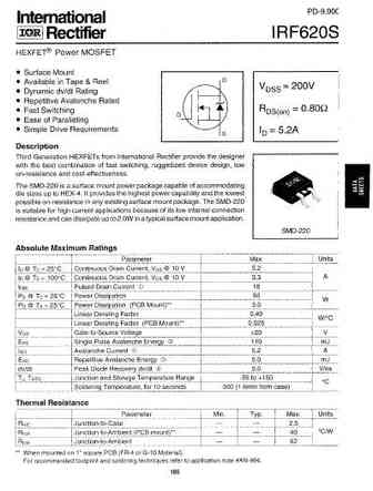
irf620spbf.pdf
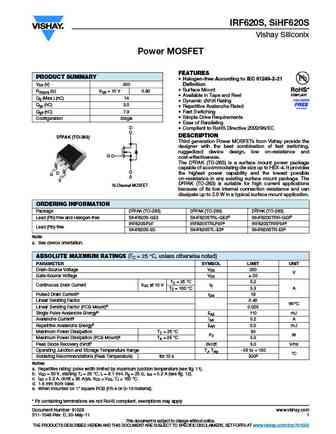
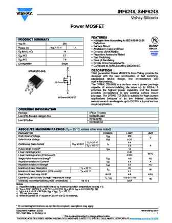
IRF620S, SiHF620S Vishay Siliconix Power MOSFET FEATURES PRODUCT SUMMARY Halogen-free According to IEC 61249-2-21 VDS (V) 200 Definition Surface Mount RDS(on) ( )VGS = 10 V 0.80 Available in Tape and Reel Qg (Max.) (nC) 14 Dynamic dV/dt Rating Qgs (nC) 3.0 Repetitive Avalanche Rated Qgd (nC) 7.9 Fast Switching Simple Drive Requirements Configuratio... See More ⇒
auirf6215s.pdf
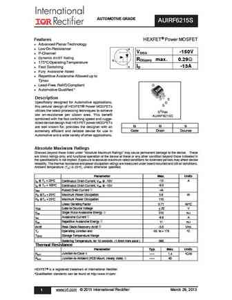
AUTOMOTIVE GRADE AUIRF6215S Features HEXFET Power MOSFET l Advanced Planar Technology l Low On-Resistance D VDSS -150V l P-Channel l Dynamic dV/dT Rating G RDS(on) max. 0.29 l 175 C Operating Temperature S ID -13A l Fast Switching l Fully Avalanche Rated l Repetitive Avalanche Allowed up to Tjmax l Lead-Free, RoHS Compliant D l Automotive Qualified * Description S Spec... See More ⇒
irf6215pbf.pdf
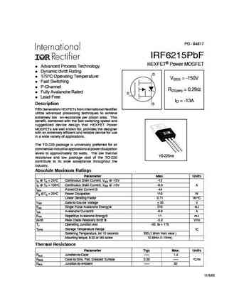
PD - 94817 IRF6215PbF HEXFET Power MOSFET Advanced Process Technology Dynamic dv/dt Rating D 175 C Operating Temperature VDSS = -150V Fast Switching P-Channel RDS(on) = 0.29 Fully Avalanche Rated G Lead-Free ID = -13A Description S Fifth Generation HEXFETs from International Rectifier utilize advanced processing techniques to achieve extremely low on-resistance pe... See More ⇒
irf620.pdf
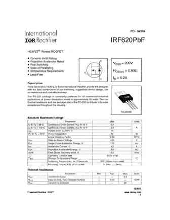
PD - 94870 IRF620PbF Lead-Free 12/5/03 Document Number 91027 www.vishay.com 1 IRF620PbF Document Number 91027 www.vishay.com 2 IRF620PbF Document Number 91027 www.vishay.com 3 IRF620PbF Document Number 91027 www.vishay.com 4 IRF620PbF Document Number 91027 www.vishay.com 5 IRF620PbF Document Number 91027 www.vishay.com 6 IRF620PbF TO-220AB Package Outline ... See More ⇒
irf6216.pdf
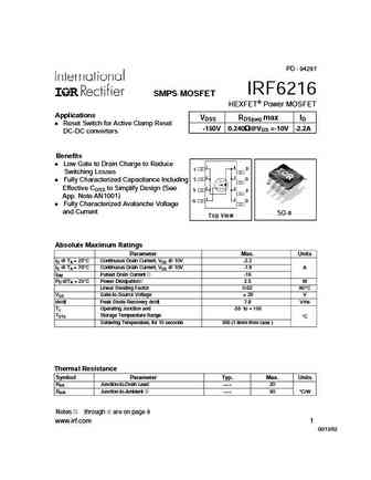
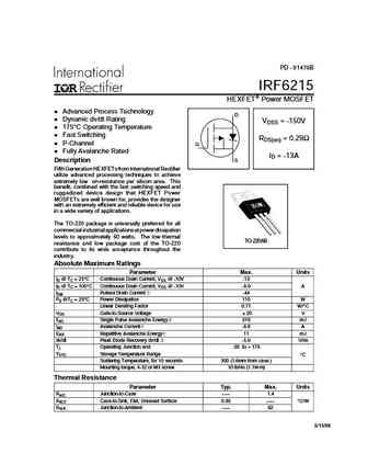
PD - 94297 IRF6216 SMPS MOSFET HEXFET Power MOSFET Applications VDSS RDS(on) max ID Reset Switch for Active Clamp Reset -150V 0.240 @VGS =-10V -2.2A DC-DC converters Benefits Low Gate to Drain Charge to Reduce A 1 8 S D Switching Losses 2 7 S D Fully Characterized Capacitance Including 3 Effective COSS to Simplify Design (See 6 S D App. Note AN1001... See More ⇒
irf624spbf.pdf
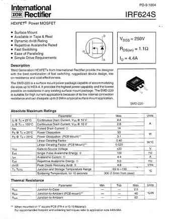
PD- 95985 IRF624SPbF Lead-Free 12/21/04 Document Number 91030 www.vishay.com 1 IRF624SPbF Document Number 91030 www.vishay.com 2 IRF624SPbF Document Number 91030 www.vishay.com 3 IRF624SPbF Document Number 91030 www.vishay.com 4 IRF624SPbF Document Number 91030 www.vishay.com 5 IRF624SPbF Document Number 91030 www.vishay.com 6 IRF624SPbF Peak Diode Recovery... See More ⇒
irf6215spbf irf6215lpbf.pdf

PD - 95132 IRF6215S/LPbF Lead-Free www.irf.com 1 4/21/05 IRF6215S/LPbF 2 www.irf.com IRF6215S/LPbF www.irf.com 3 IRF6215S/LPbF 4 www.irf.com IRF6215S/LPbF www.irf.com 5 IRF6215S/LPbF 6 www.irf.com IRF6215S/LPbF www.irf.com 7 IRF6215S/LPbF D2Pak Package Outline D2Pak Part Marking Information THIS IS AN IRF530S WIT H PART NUMBER LOT CODE 8024 INTERNAT IONAL AS S... See More ⇒
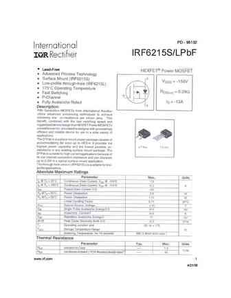
irf6215.pdf
PD - 91479B IRF6215 HEXFET Power MOSFET Advanced Process Technology D Dynamic dv/dt Rating VDSS = -150V 175 C Operating Temperature Fast Switching RDS(on) = 0.29 P-Channel G Fully Avalanche Rated ID = -13A Description S Fifth Generation HEXFETs from International Rectifier utilize advanced processing techniques to achieve extremely low on-resistance per silicon area... See More ⇒
auirf6218l auirf6218s.pdf
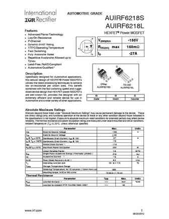
AUTOMOTIVE GRADE AUIRF6218S AUIRF6218L Features HEXFET Power MOSFET l Advanced Planar Technology l Low On-Resistance D V(BR)DSS -150V l P-Channel l Dynamic dV/dT Rating RDS(on) max 150m l 175 C Operating Temperature G l Fast Switching S ID -27A l Fully Avalanche Rated l Repetitive Avalanche Allowed up to Tjmax l Lead-Free, RoHS Compliant D l Automotive Qualified * D ... See More ⇒
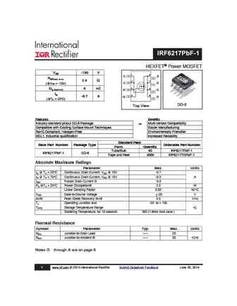
irf6216pbf-1.pdf
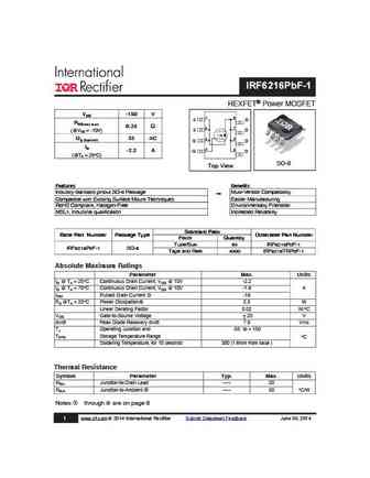
IRF6216PbF-1 HEXFET Power MOSFET VDS -150 V A 1 8 S D RDS(on) max 0.24 2 7 S D (@V = -10V) GS Qg (typical) 33 nC 3 6 S D ID 4 5 -2.2 A G D (@T = 25 C) A SO-8 Top View Features Benefits Industry-standard pinout SO-8 Package Multi-Vendor Compatibility Compatible with Existing Surface Mount Techniques Easier Manufacturing RoHS Compliant, Halogen-Free Environme... See More ⇒
irf624.pdf
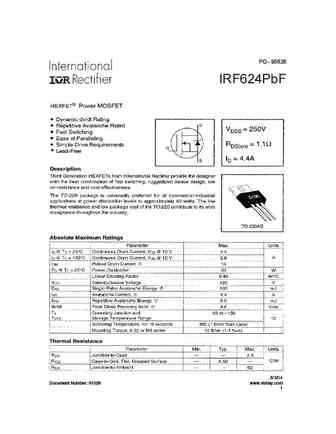
PD - 95626 IRF624PbF Lead-Free 8/3/04 Document Number 91029 www.vishay.com 1 IRF624PbF Document Number 91029 www.vishay.com 2 IRF624PbF Document Number 91029 www.vishay.com 3 IRF624PbF Document Number 91029 www.vishay.com 4 IRF624PbF Document Number 91029 www.vishay.com 5 IRF624PbF Document Number 91029 www.vishay.com 6 IRF624PbF Document Number 91029 www.... See More ⇒
irf6201pbf.pdf
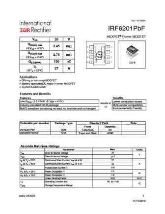
PD - 97500A IRF6201PbF HEXFET Power MOSFET VDS 20 V RDS(on) max 2.45 m (@VGS = 4.5V) RDS(on) max 2.75 m (@VGS = 2.5V) Qg (typical) 130 nC SO-8 ID 27 A (@TA = 25 C) Applications OR-ing or hot-swap MOSFET Battery operated DC motor inverter MOSFET System/Load switch Features and Benefits Features Benefits Low RDSon ( 2.45m @ Vgs = 4.5V) Lower ... See More ⇒

irf620pbf.pdf
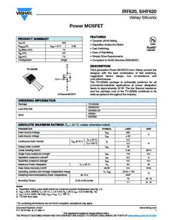
IRF620, SiHF620 Vishay Siliconix Power MOSFET FEATURES PRODUCT SUMMARY Dynamic dV/dt Rating VDS (V) 200 Available Repetitive Avalanche Rated RDS(on) ( )VGS = 10 V 0.80 RoHS* Fast Switching Qg (Max.) (nC) 14 COMPLIANT Ease of Paralleling Qgs (nC) 3.0 Qgd (nC) 7.9 Simple Drive Requirements Configuration Single Compliant to RoHS Directive 2002/95/EC D ... See More ⇒
irf6217.pdf
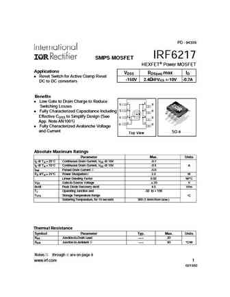
PD - 94359 IRF6217 SMPS MOSFET HEXFET Power MOSFET Applications VDSS RDS(on) max ID Reset Switch for Active Clamp Reset -150V 2.4 @VGS =-10V -0.7A DC to DC converters Benefits Low Gate to Drain Charge to Reduce A 1 8 S D Switching Losses 2 7 S D Fully Characterized Capacitance Including 3 6 Effective COSS to Simplify Design (See S D App. Note AN100... See More ⇒
irf6217pbf-1.pdf
IRF6217PbF-1 HEXFET Power MOSFET VDS -150 V A 1 8 S D RDS(on) max 2.4 2 7 S D (@V = -10V) GS Qg (typical) 6 nC 3 6 S D ID 4 5 -0.7 A G D (@T = 25 C) A SO-8 Top View Features Benefits Industry-standard pinout SO-8 Package Multi-Vendor Compatibility Compatible with Existing Surface Mount Techniques Easier Manufacturing RoHS Compliant, Halogen-Free Environment... See More ⇒
irf6218pbf.pdf
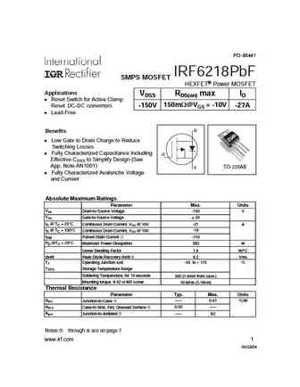
PD -95441 IRF6218PbF SMPS MOSFET HEXFET Power MOSFET Applications VDSS RDS(on) max ID l Reset Switch for Active Clamp 150m @VGS = -10V -27A -150V Reset DC-DC converters l Lead-Free D Benefits l Low Gate to Drain Charge to Reduce Switching Losses l Fully Characterized Capacitance Including G Effective COSS to Simplify Design (See App. Note AN1001) TO-220AB S l Fully Charac... See More ⇒
irf6217pbf.pdf
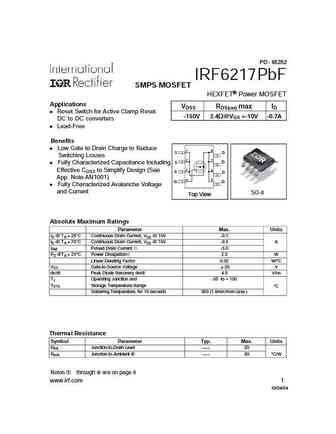
PD - 95252 IRF6217PbF SMPS MOSFET HEXFET Power MOSFET Applications VDSS RDS(on) max ID l Reset Switch for Active Clamp Reset -150V 2.4W@VGS =-10V -0.7A DC to DC converters l Lead-Free Benefits l Low Gate to Drain Charge to Reduce A 1 8 S D Switching Losses 2 7 S D l Fully Characterized Capacitance Including 3 6 Effective COSS to Simplify Design (See S D App. Note AN1001) ... See More ⇒
irf6215lpbf irf6215spbf.pdf
PD - 95132 IRF6215S/LPbF Lead-Free www.irf.com 1 4/21/05 IRF6215S/LPbF 2 www.irf.com IRF6215S/LPbF www.irf.com 3 IRF6215S/LPbF 4 www.irf.com IRF6215S/LPbF www.irf.com 5 IRF6215S/LPbF 6 www.irf.com IRF6215S/LPbF www.irf.com 7 IRF6215S/LPbF D2Pak Package Outline D2Pak Part Marking Information THIS IS AN IRF530S WIT H PART NUMBER LOT CODE 8024 INTERNAT IONAL AS S... See More ⇒
irf620.pdf
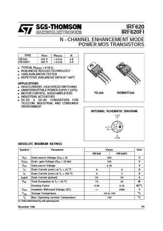
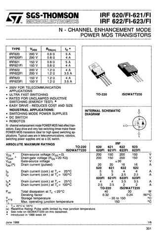
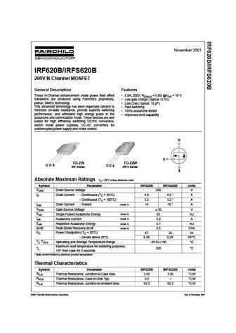
IRF620 IRF620FI N - CHANNEL ENHANCEMENT MODE POWER MOS TRANSISTORS TYPE VDSS RDS(on) ID IRF620 200 V ... See More ⇒
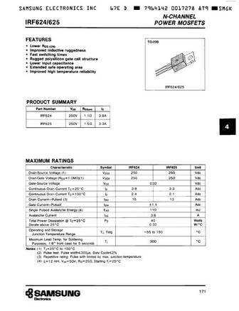
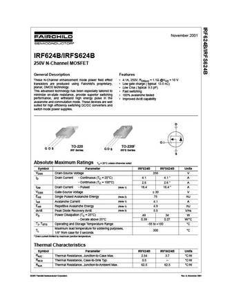
irf624b irfs624b.pdf

November 2001 IRF624B/IRFS624B 250V N-Channel MOSFET General Description Features These N-Channel enhancement mode power field effect 4.1A, 250V, RDS(on) = 1.1 @VGS = 10 V transistors are produced using Fairchild s proprietary, Low gate charge ( typical 13.5 nC) planar, DMOS technology. Low Crss ( typical 9.5 pF) This advanced technology has been especially tailored to ... See More ⇒
irf624a.pdf
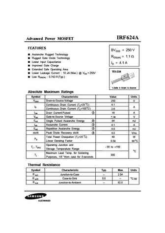
Advanced Power MOSFET FEATURES BVDSS = 250 V Avalanche Rugged Technology RDS(on) = 1.1 Rugged Gate Oxide Technology Lower Input Capacitance ID = 4.1 A Improved Gate Charge Extended Safe Operating Area Lower Leakage Current 10 A (Max.) @ VDS = 250V Low RDS(ON) 0.742 (Typ.) 1 2 3 1.Gate 2. Drain 3. Source Absolute Maximum Ratings Symbol Characteristic Val... See More ⇒
irf620a.pdf

Advanced Power MOSFET FEATURES BVDSS = 200 V Avalanche Rugged Technology RDS(on) = 0.8 Rugged Gate Oxide Technology Lower Input Capacitance ID = 5 A Improved Gate Charge Extended Safe Operating Area Lower Leakage Current 10 A (Max.) @ VDS = 200V Low RDS(ON) 0.626 (Typ.) 1 2 3 1.Gate 2. Drain 3. Source Absolute Maximum Ratings Symbol Characteristic Value ... See More ⇒
irf624 sihf624.pdf
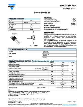
IRF624, SiHF624 Vishay Siliconix Power MOSFET FEATURES PRODUCT SUMMARY Dynamic dV/dt Rating VDS (V) 250 Available Repetitive Avalanche Rated RDS(on) ( )VGS = 10 V 1.1 RoHS* Fast Switching Qg (Max.) (nC) 14 COMPLIANT Ease of Paralleling Qgs (nC) 2.7 Simple Drive Requirements Qgd (nC) 7.8 Configuration Single Compliant to RoHS Directive 2002/95/EC D DE... See More ⇒
irf624pbf sihf624.pdf

IRF624, SiHF624 Vishay Siliconix Power MOSFET FEATURES PRODUCT SUMMARY Dynamic dV/dt Rating VDS (V) 250 Available Repetitive Avalanche Rated RDS(on) ( )VGS = 10 V 1.1 RoHS* Fast Switching Qg (Max.) (nC) 14 COMPLIANT Ease of Paralleling Qgs (nC) 2.7 Simple Drive Requirements Qgd (nC) 7.8 Configuration Single Compliant to RoHS Directive 2002/95/EC D DE... See More ⇒
irf624spbf sihf624s.pdf
IRF624S, SiHF624S Vishay Siliconix Power MOSFET FEATURES PRODUCT SUMMARY Halogen-free According to IEC 61249-2-21 Definition VDS (V) 250 Surface Mount RDS(on) ( )VGS = 10 V 1.1 Available in Tape and Reel Qg (Max.) (nC) 14 Dynamic dV/dt Rating Repetitive Avalanche Rated Qgs (nC) 2.7 Fast Switching Qgd (nC) 7.8 Ease of Paralleling Simple Drive R... See More ⇒
irf620 sihf620.pdf

IRF620, SiHF620 Vishay Siliconix Power MOSFET FEATURES PRODUCT SUMMARY Dynamic dV/dt Rating VDS (V) 200 Available Repetitive Avalanche Rated RDS(on) ( )VGS = 10 V 0.80 RoHS* Fast Switching Qg (Max.) (nC) 14 COMPLIANT Ease of Paralleling Qgs (nC) 3.0 Qgd (nC) 7.9 Simple Drive Requirements Configuration Single Compliant to RoHS Directive 2002/95/EC D ... See More ⇒
irf6218spbf.pdf
SMPS MOSFET IRF6218SPbF HEXFET Power MOSFET Applications VDSS RDS(on) (max) ID Reset Switch for Active Clamp Reset DC-DC converters - 150V 150m @ VGS = -10V -27A Benefits D Low Gate to Drain Charge to Reduce Switching Losses Fully Characterized Capacitance Including Effective COSS to Simplify Design (See App. Note AN1001) S Fully Characterized... See More ⇒
auirf6215s.pdf
AUTOMOTIVE GRADE AUIRF6215S HEXFET Power MOSFET Features Advanced Planar Technology VDSS -150V Low On-Resistance P-Channel MOSFET RDS(on) max. 0.29 Dynamic dv/dt Rating 175 C Operating Temperature ID -13A Fast Switching Fully Avalanche Rated D Repetitive Avalanche Allowed up to Tjmax Lead-Free, RoHS Compliant Automo... See More ⇒
irf6218.pdf
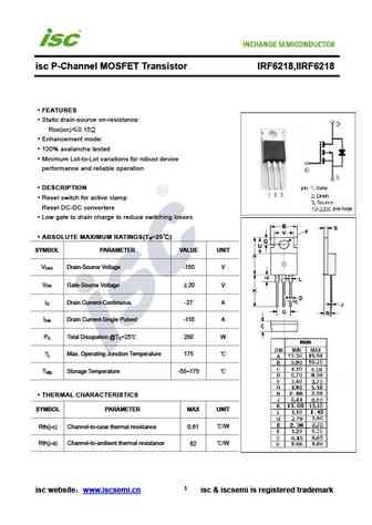
isc P-Channel MOSFET Transistor IRF6218,IIRF6218 FEATURES Static drain-source on-resistance RDS(on) 0.15 Enhancement mode 100% avalanche tested Minimum Lot-to-Lot variations for robust device performance and reliable operation DESCRIPTION Reset switch for active clamp Reset DC-DC converters Low gate to drain charge to reduce switching losses ABSOLUTE MAXIMUM... See More ⇒
Detailed specifications: IRF532FI, IRF533FI, IRF541FI, IRF542FI, IRF543FI, IRF621FI, IRF622FI, IFR623, AON7410, IRF721FI, IRF722FI, IRF723FI, IRF731FI, IRF732FI, IRF733FI, IRF741FI, IRF742FI
Keywords - IRF623FI MOSFET specs
IRF623FI cross reference
IRF623FI equivalent finder
IRF623FI pdf lookup
IRF623FI substitution
IRF623FI replacement
Learn how to find the right MOSFET substitute. A guide to cross-reference, check specs and replace MOSFETs in your circuits.
History: RU30J30M | SI4953ADY-T1-E3 | STW35N65DM2 | VS6808DH | FDD9407 | KI007P | 2SK2402
🌐 : EN ES РУ

LIST
Last Update
MOSFET: AUB034N10 | AUB033N08BG | AUB026N085 | AUA062N08BG | AUA060N08AG | AUA056N08BGL | AUA039N10 | ASW80R290E | ASW65R120EFD | ASW65R110E
Popular searches
irf1404 | bc550 | irf9530 | 2n2222a transistor | irfp250 | irf640n datasheet | irf540 datasheet | irf530