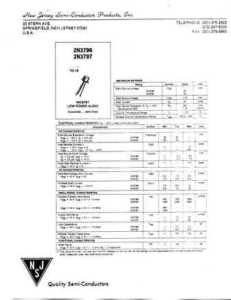
2N3796 Specs and Replacement
Type Designator: 2N3796
Type of Transistor: MOSFET
Type of Control Channel: N-Channel
Absolute Maximum Ratings
Pd ⓘ
- Maximum Power Dissipation: 0.2 W
|Vds|ⓘ - Maximum Drain-Source Voltage: 25 V
|Vgs|ⓘ - Maximum Gate-Source Voltage: 10 V
|Id| ⓘ - Maximum Drain Current: 0.02 A
Tj ⓘ - Maximum Junction Temperature: 175 °C
Electrical Characteristics
Package: TO-18
TO-206AA
- MOSFET ⓘ Cross-Reference Search
2N3796 datasheet
9.3. Size:223K motorola
2n3791 2n3792.pdf 
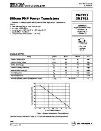
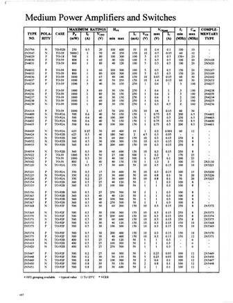
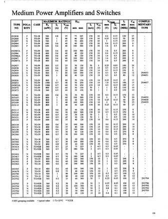
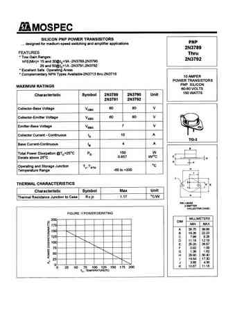
Order this document MOTOROLA by 2N3791/D SEMICONDUCTOR TECHNICAL DATA 2N3791 Silicon PNP Power Transistors 2N3792 . . . designed for medium speed switching and amplifier applications. These devices feature 10 AMPERE Total Switching Time @ 3.0 A [ 1.0 s (typ) POWER TRANSISTORS hFE (min) = 50 @ 1.0 A PNP SILICON Low VCE(sat) = 0.5 V (typ) @ IC = 5.0 A, IB = 0.5 A 60... See More ⇒
9.4. Size:122K central
2n3789 2n3790 2n3791 2n3792.pdf
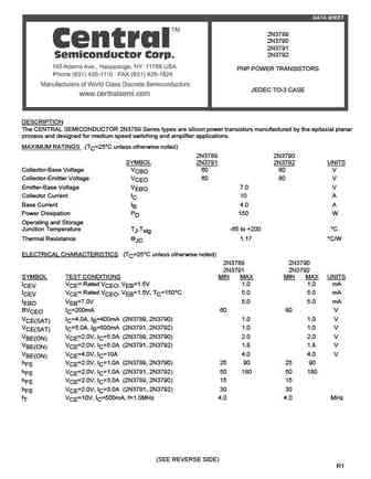
DATA SHEET 2N3789 2N3790 2N3791 2N3792 PNP POWER TRANSISTORS JEDEC TO-3 CASE DESCRIPTION The CENTRAL SEMICONDUCTOR 2N3789 Series types are silicon power transistors manufactured by the epitaxial planar process and designed for medium speed switching and amplifier applications. MAXIMUM RATINGS (TC=25 C unless otherwise noted) 2N3789 2N3790 SYMBOL 2N3791 2N3792 UNITS Col... See More ⇒
9.5. Size:172K comset
2n3713-2n3714-2n3715-2n3716-2n3789-2n3790-2n3791-2n3792.pdf
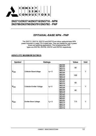
2N3713/2N3714/2N3715/2N3716 - NPN 2N3789/2N3790/2N3791/2N3792 - PNP EPITAXIAL-BASE NPN - PNP The 2N3713, 2N3714, 2N3715 and 2N3716 are silicon epitaxial-base NPN power transistor in Jedec TO-3 metal case. They are inteded for use in power linear and switching applications. The complementary PNP types are 2N3789, 2N3790, 2N3791 and 2N3792 respectively. ABSOLUTE MAXIMUM RATINGS Symbol Rat... See More ⇒
9.7. Size:27K semelab
2n3799.pdf
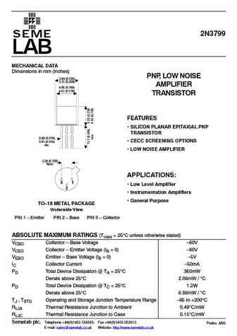
2N3799 SEME LAB MECHANICAL DATA Dimensions in mm (inches) PNP, LOW NOISE 5.84 (0.230) 5.31 (0.209) AMPLIFIER 4.95 (0.195) 4.52 (0.178) TRANSISTOR FEATURES SILICON PLANAR EPITAXIAL PNP TRANSISTOR 0.48 (0.019) 0.41 (0.016) CECC SCREENING OPTIONS dia. LOW NOISE AMPLIFIER 2.54 (0.100) Nom. APPLICATIONS 3 1 Low Level Amplifier 2 Instrumentation Amplifier... See More ⇒
9.8. Size:10K semelab
2n3790smd.pdf

2N3790SMD Dimensions in mm (inches). Bipolar PNP Device in a Hermetically sealed 0.89 (0.035) min. Ceramic Surface Mount 3.70 (0.146) 3.70 (0.146) 3.60 (0.142) 3.41 (0.134) 3.41 (0.134) Max. Package for High Reliability Applications 1 3 Bipolar PNP Device. 2 VCEO = 80V IC = 10A 9.67 (0.381) All Semelab hermetically sealed products 9.38 (0.369) 0.50 (0.020) 0.26 (... See More ⇒
9.9. Size:10K semelab
2n3790xsmd.pdf

2N3790XSMD Dimensions in mm (inches). Bipolar PNP Device in a Hermetically sealed 0.89 (0.035) min. Ceramic Surface Mount 3.70 (0.146) 3.70 (0.146) 3.60 (0.142) 3.41 (0.134) 3.41 (0.134) Max. Package for High Reliability Applications 1 3 Bipolar PNP Device. 2 VCEO = 80V IC = 10A 9.67 (0.381) All Semelab hermetically sealed products 9.38 (0.369) 0.50 (0.020) 0.26 ... See More ⇒
9.10. Size:10K semelab
2n3792smd.pdf

2N3792SMD Dimensions in mm (inches). Bipolar PNP Device in a Hermetically sealed 0.89 (0.035) min. Ceramic Surface Mount 3.70 (0.146) 3.70 (0.146) 3.60 (0.142) 3.41 (0.134) 3.41 (0.134) Max. Package for High Reliability Applications 1 3 Bipolar PNP Device. 2 VCEO = 80V IC = 10A 9.67 (0.381) All Semelab hermetically sealed products 9.38 (0.369) 0.50 (0.020) 0.26 (... See More ⇒
9.11. Size:10K semelab
2n3791smd.pdf
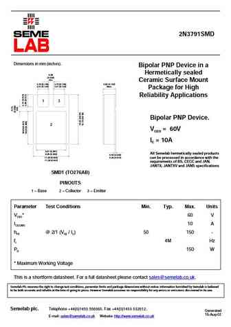
2N3791SMD Dimensions in mm (inches). Bipolar PNP Device in a Hermetically sealed 0.89 (0.035) min. Ceramic Surface Mount 3.70 (0.146) 3.70 (0.146) 3.60 (0.142) 3.41 (0.134) 3.41 (0.134) Max. Package for High Reliability Applications 1 3 Bipolar PNP Device. 2 VCEO = 60V IC = 10A 9.67 (0.381) All Semelab hermetically sealed products 9.38 (0.369) 0.50 (0.020) 0.26 (... See More ⇒
9.12. Size:130K inchange semiconductor
2n3791 2n3792.pdf
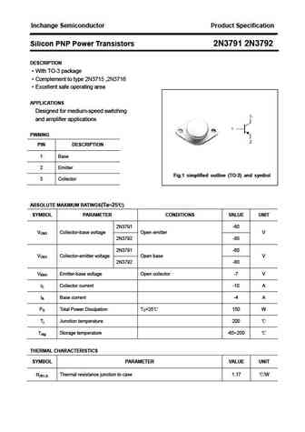
Inchange Semiconductor Product Specification Silicon PNP Power Transistors 2N3791 2N3792 DESCRIPTION With TO-3 package Complement to type 2N3715 ,2N3716 Excellent safe operating area APPLICATIONS Designed for medium-speed switching and amplifier applications PINNING PIN DESCRIPTION 1 Base 2 Emitter Fig.1 simplified outline (TO-3) and symbol 3 Collector ABSOLUTE M... See More ⇒
9.13. Size:184K inchange semiconductor
2n3790.pdf
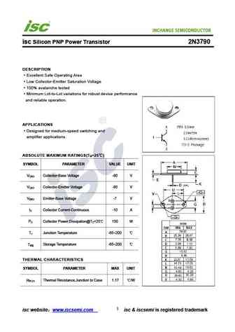
isc Silicon PNP Power Transistor 2N3790 DESCRIPTION Excellent Safe Operating Area Low Collector-Emitter Saturation Voltage 100% avalanche tested Minimum Lot-to-Lot variations for robust device performance and reliable operation. APPLICATIONS Designed for medium-speed switching and amplifier applications. ABSOLUTE MAXIMUM RATINGS(T =25 ) a SYMBOL PARAMETER VALUE UNIT V C... See More ⇒
9.14. Size:191K inchange semiconductor
2n3792.pdf

INCHANGE Semiconductor isc Silicon PNP Power Transistor 2N3792 DESCRIPTION Excellent Safe Operating Area Low Collector-Emitter Saturation Voltage 100% tested Minimum Lot-to-Lot variations for robust device performance and reliable operation. APPLICATIONS Designed for medium-speed switching and amplifier applications. ABSOLUTE MAXIMUM RATINGS(T =25 ) a SYMBOL PARAMETER V... See More ⇒
Detailed specifications: 3SK318
, 3SK324
, 2N2608
, 2N2609
, 2N3684
, 2N3685
, 2N3686
, 2N3687
, K3569
, 2N3797
, 2N3820
, 2N3821
, 2N3822
, 2N3823
, 2N3921
, 2N3922
, 2N3954
.
Keywords - 2N3796 MOSFET specs
2N3796 cross reference
2N3796 equivalent finder
2N3796 pdf lookup
2N3796 substitution
2N3796 replacement
Need a MOSFET replacement?
Our guide shows you how to find a perfect substitute by comparing key parameters and specs