10N90 Specs and Replacement
Type Designator: 10N90
Type of Transistor: MOSFET
Type of Control Channel: N -Channel
Absolute Maximum Ratings
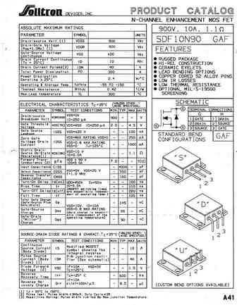
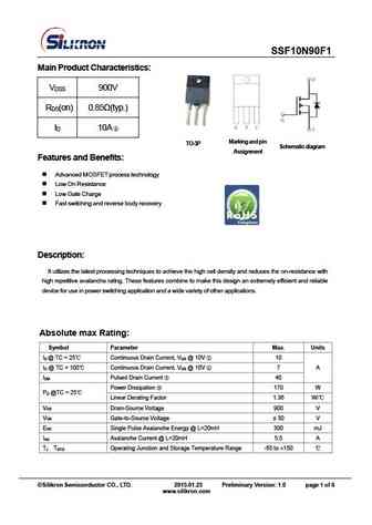
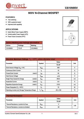
Pd ⓘ - Maximum Power Dissipation: 183 W
|Vds|ⓘ - Maximum Drain-Source Voltage: 900 V
|Vgs|ⓘ - Maximum Gate-Source Voltage: 30 V
|Id| ⓘ - Maximum Drain Current: 10 A
Tj ⓘ - Maximum Junction Temperature: 150 °C
Electrical Characteristics
tr ⓘ - Rise Time: 54 nS
Cossⓘ - Output Capacitance: 245 pF
Rds ⓘ - Maximum Drain-Source On-State Resistance: 1.15 Ohm
Package: TO-247 TO-3P
10N90 substitution
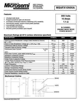
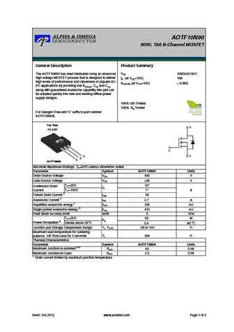
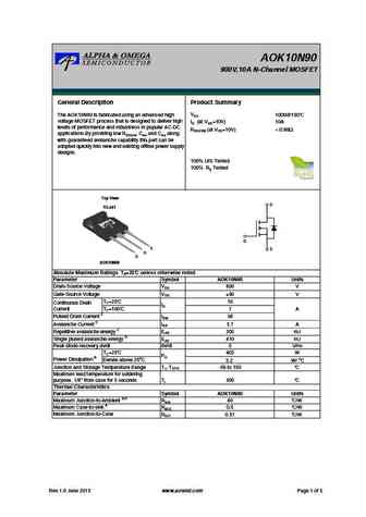
10N90 datasheet
10n90.pdf
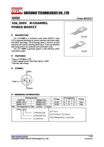
UNISONIC TECHNOLOGIES CO., LTD 10N90 Power MOSFET 10A, 900V N-CHANNEL POWER MOSFET DESCRIPTION The UTC10N90 is a N-channel mode power MOSFET using UTC s advanced technology to provide costumers with planar stripe and DMOS technology. This technology allows a minimum on-state resistance and superior switching performance. It also can withstand high energy pulse in the avalan... See More ⇒
ssf10n90a.pdf
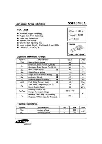
Advanced Power MOSFET FEATURES BVDSS = 900 V Avalanche Rugged Technology RDS(on) = 1.2 Rugged Gate Oxide Technology Lower Input Capacitance ID = 6.5 A Improved Gate Charge Extended Safe Operating Area Lower Leakage Current 25 A (Max.) @ VDS = 900V Low RDS(ON) 0.938 (Typ.) 1 2 3 1.Gate 2. Drain 3. Source Absolute Maximum Ratings Symbol Characteristic Valu... See More ⇒
ssh10n90a.pdf
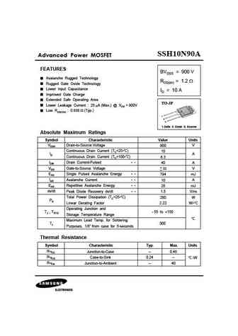
SSH10N90A Advanced Power MOSFET FEATURES BVDSS = 900 V Avalanche Rugged Technology RDS(on) = 1.2 Rugged Gate Oxide Technology Lower Input Capacitance ID = 10 A Improved Gate Charge Extended Safe Operating Area TO-3P Lower Leakage Current 25 A (Max.) @ VDS = 900V Low RDS(ON) 0.938 (Typ.) 1 2 3 1.Gate 2. Drain 3. Source Absolute Maximum Ratings Symbol Char... See More ⇒
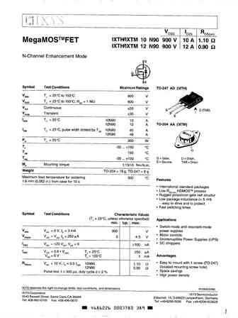
ixfh10n90 ixfm10n90 ixfh12n90 ixfm12n90 ixfh13n90 ixfm13n90.pdf
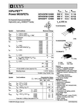
VDSS ID25 RDS(on) HiPerFETTM IXFH/IXFM 10 N90 900 V 10 A 1.1 Power MOSFETs IXFH/IXFM 12 N90 900 V 12 A 0.9 IXFH/IXFT 13 N90 900 V 13 A 0.8 N-Channel Enhancement Mode 250 ns High dv/dt, Low trr, HDMOSTM Family trr TO-247 AD (IXFH) Symbol Test Conditions Maximum Ratings VDSS TJ = 25 C to 1... See More ⇒
Detailed specifications: STK004SF , SUF1002 , SUF2001 , SUF3001 , SUM201MN , SUM202MN , 8N90 , 9N90 , IRFB4110 , 11N90 , 12N90 , 9N95 , 9N100 , 1N90 , 2N90 , 3N90 , 4N90 .
Keywords - 10N90 MOSFET specs
10N90 cross reference
10N90 equivalent finder
10N90 pdf lookup
10N90 substitution
10N90 replacement
Need a MOSFET replacement? Our guide shows you how to find a perfect substitute by comparing key parameters and specs


LIST
Last Update
MOSFET: AOK065V65X2 | AOK065V120X2 | AOK033V120X2Q | AOK033V120X2 | AOB380A60L | AOB29S50L | AO3481C | AO3480 | APG068N04Q | APG068N04G
Popular searches
2sc2625 | 2sc1815 transistor | 2sd718 | 2n3053 transistor | 2sc458 replacement | bc557 transistor | 2n3638 | tip127 datasheet
