5N90 Specs and Replacement
Type Designator: 5N90
Type of Transistor: MOSFET
Type of Control Channel: N-Channel
Absolute Maximum Ratings
Pd ⓘ
- Maximum Power Dissipation: 240 W
|Vds|ⓘ - Maximum Drain-Source Voltage: 900 V
|Vgs|ⓘ - Maximum Gate-Source Voltage: 30 V
|Id| ⓘ - Maximum Drain Current: 5 A
Tj ⓘ - Maximum Junction Temperature: 150 °C
Electrical Characteristics
tr ⓘ - Rise Time: 65 nS
Cossⓘ -
Output Capacitance: 110 pF
RDSonⓘ - Maximum Drain-Source On-State Resistance: 2.25 Ohm
Package: TO-3P
TO-220F1
TO-220
TO-262
- MOSFET ⓘ Cross-Reference Search
5N90 datasheet
..1. Size:257K utc
5n90.pdf 
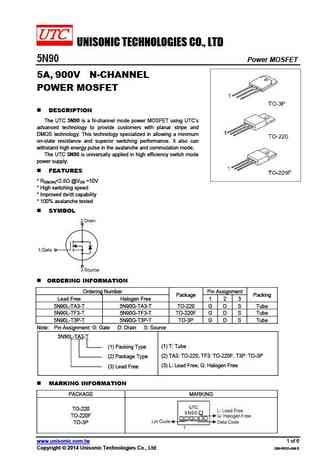
UNISONIC TECHNOLOGIES CO., LTD 5N90 Power MOSFET 5A, 900V N-CHANNEL POWER MOSFET DESCRIPTION The UTC 5N90 is a N-channel mode power MOSFET using UTC s advanced technology to provide customers with planar stripe and DMOS technology. This technology specialized in allowing a minimum on-state resistance and superior switching performance. It also can withstand high energy p... See More ⇒
0.2. Size:396K 1
sgf15n90d.pdf
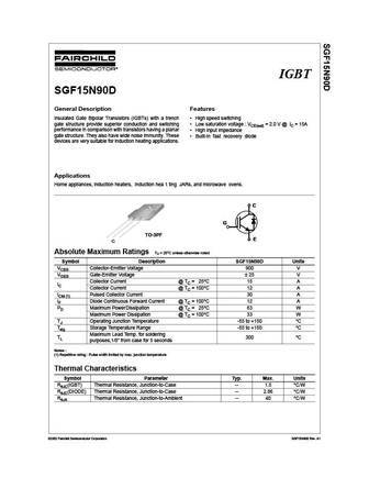
IGBT SGF15N90D General Description Features Insulated Gate Bipolar Transistors (IGBTs) with a trench High speed switching gate structure provide superior conduction and switching Low saturation voltage VCE(sat) = 2.0 V @ IC = 15A performance in comparison with transistors having a planar High input impedance gate structure. They also have wide noise immunity. These Bu... See More ⇒
0.6. Size:619K fairchild semi
fqa5n90.pdf
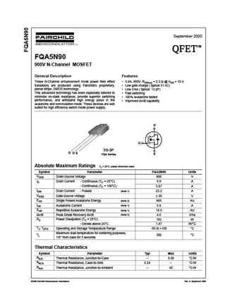
September 2000 TM QFET QFET QFET QFET FQA5N90 900V N-Channel MOSFET General Description Features These N-Channel enhancement mode power field effect 5.8A, 900V, RDS(on) = 2.3 @ VGS = 10 V transistors are produced using Fairchild s proprietary, Low gate charge ( typical 31 nC) planar stripe, DMOS technology. Low Crss ( typical 13 pF) This advanced technology has be... See More ⇒
0.7. Size:678K fairchild semi
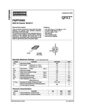
fqp5n90.pdf
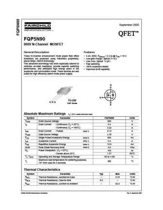
September 2000 TM QFET QFET QFET QFET FQP5N90 900V N-Channel MOSFET General Description Features These N-Channel enhancement mode power field effect 5.4A, 900V, RDS(on) = 2.3 @ VGS = 10 V transistors are produced using Fairchild s proprietary, Low gate charge ( typical 31 nC) planar stripe, DMOS technology. Low Crss ( typical 13 pF) This advanced technology has be... See More ⇒
0.8. Size:1029K fairchild semi
fqb5n90tm.pdf
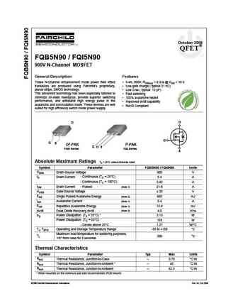
October 2008 QFET FQB5N90 / FQI5N90 900V N-Channel MOSFET General Description Features These N-Channel enhancement mode power field effect 5.4A, 900V, RDS(on) = 2.3 @ VGS = 10 V transistors are produced using Fairchild s proprietary, Low gate charge ( typical 31 nC) planar stripe, DMOS technology. Low Crss ( typical 13 pF) This advanced technology has been especiall... See More ⇒
0.9. Size:1072K fairchild semi
fqb5n90 fqi5n90.pdf

October 2008 QFET FQB5N90 / FQI5N90 900V N-Channel MOSFET General Description Features These N-Channel enhancement mode power field effect 5.4A, 900V, RDS(on) = 2.3 @ VGS = 10 V transistors are produced using Fairchild s proprietary, Low gate charge ( typical 31 nC) planar stripe, DMOS technology. Low Crss ( typical 13 pF) This advanced technology has been especiall... See More ⇒
0.10. Size:660K fairchild semi
fqaf5n90.pdf
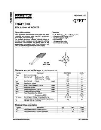
September 2000 TM QFET QFET QFET QFET FQAF5N90 900V N-Channel MOSFET General Description Features These N-Channel enhancement mode power field effect 4.1A, 900V, RDS(on) = 2.3 @ VGS = 10 V transistors are produced using Fairchild s proprietary, Low gate charge ( typical 31 nC) planar stripe, DMOS technology. Low Crss ( typical 13 pF) This advanced technology has b... See More ⇒
0.11. Size:665K fairchild semi
fqpf5n90.pdf
September 2000 TM QFET QFET QFET QFET FQPF5N90 900V N-Channel MOSFET General Description Features These N-Channel enhancement mode power field effect 3.0A, 900V, RDS(on) = 2.3 @ VGS = 10 V transistors are produced using Fairchild s proprietary, Low gate charge ( typical 31 nC) planar stripe, DMOS technology. Low Crss ( typical 13 pF) This advanced technology has b... See More ⇒
0.12. Size:625K fairchild semi
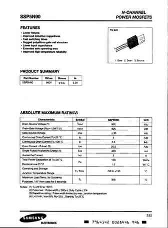
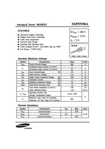
ssp5n90a.pdf
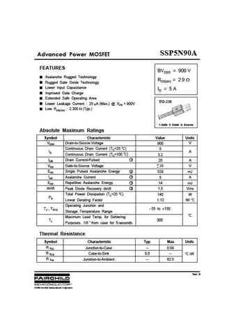
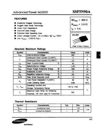
SSP5N90A Advanced Power MOSFET FEATURES BVDSS = 900 V Avalanche Rugged Technology RDS(on) = 2.9 Rugged Gate Oxide Technology Lower Input Capacitance ID = 5 A Improved Gate Charge Extended Safe Operating Area TO-220 Lower Leakage Current 25 A (Max.) @ VDS = 900V Low RDS(ON) 2.300 (Typ.) 1 2 3 1.Gate 2. Drain 3. Source Absolute Maximum Ratings Symbol Chara... See More ⇒
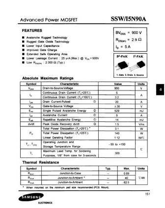
0.13. Size:934K samsung
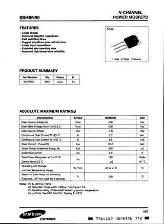
ssh5n90a.pdf
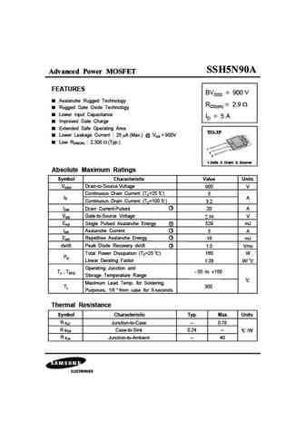
Advanced Power MOSFET FEATURES BVDSS = 900 V Avalanche Rugged Technology RDS(on) = 2.9 Rugged Gate Oxide Technology Lower Input Capacitance ID = 5 A Improved Gate Charge Extended Safe Operating Area Lower Leakage Current 25 A (Max.) @ VDS = 900V Low RDS(ON) 2.300 (Typ.) 1 2 3 1.Gate 2. Drain 3. Source Absolute Maximum Ratings Symbol Characteristic Value ... See More ⇒
0.15. Size:499K samsung
sss5n90a.pdf
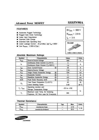
Advanced Power MOSFET FEATURES BVDSS = 900 V Avalanche Rugged Technology RDS(on) = 2.9 Rugged Gate Oxide Technology Lower Input Capacitance ID = 3 A Improved Gate Charge Extended Safe Operating Area Lower Leakage Current 25 A (Max.) @ VDS = 900V Low RDS(ON) 2.300 (Typ.) 1 2 3 1.Gate 2. Drain 3. Source Absolute Maximum Ratings Symbol Characteristic Value ... See More ⇒
0.16. Size:856K samsung
ssp5n90a.pdf
Advanced Power MOSFET FEATURES BVDSS = 900 V Avalanche Rugged Technology RDS(on) = 2.9 Rugged Gate Oxide Technology Lower Input Capacitance ID = 5 A Improved Gate Charge Extended Safe Operating Area Lower Leakage Current 25 A (Max.) @ VDS = 900V Low RDS(ON) 2.300 (Typ.) 1 2 3 1.Gate 2. Drain 3. Source Absolute Maximum Ratings Symbol Characteristic Value ... See More ⇒
0.17. Size:251K ixys
ixfk26n90 ixfx26n90 ixfk25n90 ixfx25n90.pdf
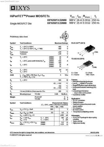
www.DataSheet4U.com VDSS IDSS RDS(on) trr HiPerFETTM Power MOSFETs IXFK/IXFX 26N90 900 V 26 A 0.30 W 250 ns IXFK/IXFX 25N90 900 V 25 A 0.33 W 250 ns Single MOSFET Die Preliminary data sheet Symbol Test Conditions Maximum Ratings PLUS 247TM (IXFX) VDSS TJ = 25 C to 150 C 900 V VDGR TJ = 25 C to 150 C; RGS = 1 MW 900 V VGS Continuous 20 V (TAB) G VGSM Transient 30 V D S ID2... See More ⇒
0.18. Size:141K ixys
ixfn26n90 ixfn25n90.pdf
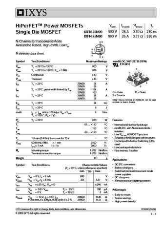
VDSS ID (cont) RDS(on) trr HiPerFETTM Power MOSFETs 900 V 26 A 0.30 W 250 ns IXFN 26N90 Single Die MOSFET IXFN 25N90 900 V 25 A 0.33 W 250 ns N-Channel Enhancement Mode D Avalanche Rated, High dv/dt, Low trr G Preliminary data sheet S S Symbol Test Conditions Maximum Ratings miniBLOC, SOT-227 B (IXFN) E153432 VDSS TJ = 25 C to 150 C 900 V S VDGR TJ = 25 C to 150 C; RGS = ... See More ⇒
0.20. Size:372K nell
5n90a 5n90af.pdf
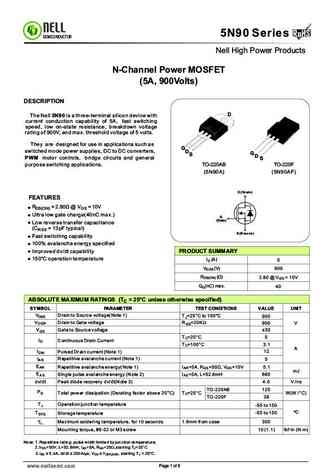
RoHS 5N90 Series RoHS SEMICONDUCTOR Nell High Power Products N-Channel Power MOSFET (5A, 900Volts) DESCRIPTION D The Nell 5N90 is a three-terminal silicon device with current conduction capability of 5A, fast switching speed, low on-state resistance, breakdown voltage rating of 900V, and max. threshold voltage of 5 volts. They are designed for use in applications such as G s... See More ⇒
0.21. Size:612K crhj
cs5n90 arh-g.pdf

Silicon N-Channel Power MOSFET R CS5N90 ARH-G General Description VDSS 900 V CS5N90 ARH-G, the silicon N-channel Enhanced ID 5 A PD(TC=25 ) 45 W VDMOSFETs, is obtained by the self-aligned planar Technology RDS(ON)Typ 2.1 which reduce the conduction loss, improve switching performance and enhance the avalanche energy. The transistor can be used in various p... See More ⇒
0.22. Size:424K crhj
cs5n90f a9h.pdf

Silicon N-Channel Power MOSFET R CS5N90F A9H General Description VDSS 900 V CS5N90F A9H, the silicon N-channel Enhanced VDMOSFETs, ID 5 A PD(TC=25 ) 45 W is obtained by the self-aligned planar Technology which reduce RDS(ON)Typ 2.1 the conduction loss, improve switching performance and enhance the avalanche energy. The transistor can be used in various power... See More ⇒
0.23. Size:124K china
cs5n90.pdf
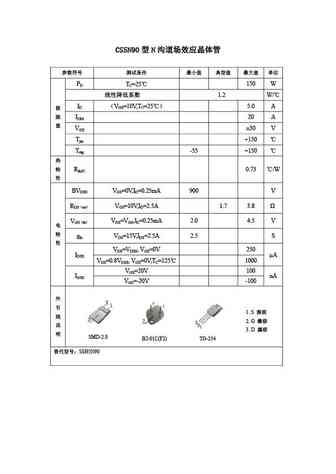
CS5N90 N PD TC=25 150 W 1.2 W/ ID VGS=10V,TC=25 5.0 A IDM 20 A VGS 30 V Tjm +150 Tstg -55 +150 RthJC 0.73 /W BVDSS VGS=0V,ID=0.25mA 900 V RDS on VGS=10V,ID=2.5A 1.7 3.8 VGS th VDS=VGS,ID=0... See More ⇒
0.24. Size:560K jiaensemi
jfpc5n90c jffm5n90c.pdf
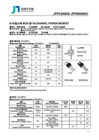
JFPC5N90C JFFM5N90C N- MOS / N-CHANNEL POWER MOSFET RoHS FEATURES LOW ON-RESISTANCE FAST SWITCHING HIGH INPUT RESISTANCE RoHS COMPLIANT APPLICATION ELECTRONIC BALLAST ELECTRONIC TRANSFORMER SWITCH MODE POWER SUP... See More ⇒
0.25. Size:788K ncepower
nce65n900i.pdf

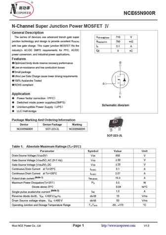
NCE65N900I N-Channel Super Junction Power MOSFET General Description The series of devices use advanced trench gate super V 710 V DS min@Tjmax junction technology and design to provide excellent RDS(ON) R 790 m DS(ON)TYP. with low gate charge. This super junction MOSFET fits the I 5.1 A D industry s AC-DC SMPS requirements for PFC, AC/DC Qg 9 nC power conversion, and indust... See More ⇒
0.26. Size:834K ncepower
nce65n900r.pdf
NCE65N900R N-Channel Super Junction Power MOSFET General Description The series of devices use advanced trench gate super V 710 V DS min@Tjmax junction technology and design to provide excellent RDS(ON) R 790 m DS(ON)TYP. with low gate charge. This super junction MOSFET fits the I 5.1 A D industry s AC-DC SMPS requirements for PFC, AC/DC Qg 9 nC power conversion, and indust... See More ⇒
0.27. Size:788K ncepower
nce65n900d.pdf

NCE65N900D N-Channel Super Junction Power MOSFET General Description The series of devices use advanced trench gate super V 710 V DS min@Tjmax junction technology and design to provide excellent RDS(ON) R 790 m DS(ON)TYP. with low gate charge. This super junction MOSFET fits the I 5.1 A D industry s AC-DC SMPS requirements for PFC, AC/DC Qg 9 nC power conversion, and indust... See More ⇒
0.28. Size:803K ncepower
nce65n900.pdf
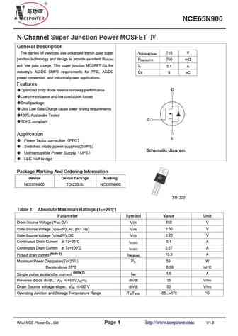
NCE65N900 N-Channel Super Junction Power MOSFET General Description The series of devices use advanced trench gate super V 710 V DS min@Tjmax junction technology and design to provide excellent RDS(ON) R 790 m DS(ON)TYP. with low gate charge. This super junction MOSFET fits the I 5.1 A D industry s AC-DC SMPS requirements for PFC, AC/DC Qg 9 nC power conversion, and industr... See More ⇒
0.29. Size:792K ncepower
nce65n900f.pdf
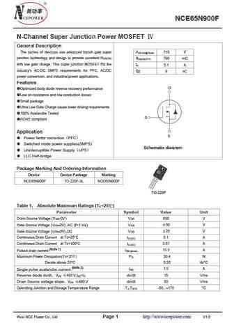
NCE65N900F N-Channel Super Junction Power MOSFET General Description The series of devices use advanced trench gate super V 710 V DS min@Tjmax junction technology and design to provide excellent RDS(ON) R 790 m DS(ON)TYP. with low gate charge. This super junction MOSFET fits the I 5.1 A D industry s AC-DC SMPS requirements for PFC, AC/DC Qg 9 nC power conversion, and indust... See More ⇒
0.30. Size:795K ncepower
nce65n900k.pdf
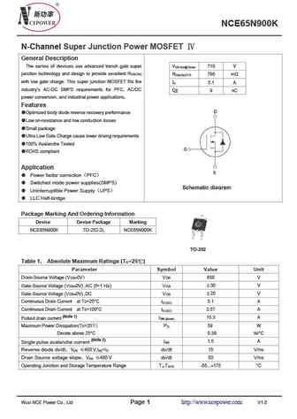
NCE65N900K N-Channel Super Junction Power MOSFET General Description The series of devices use advanced trench gate super V 710 V DS min@Tjmax junction technology and design to provide excellent RDS(ON) R 790 m DS(ON)TYP. with low gate charge. This super junction MOSFET fits the I 5.1 A D industry s AC-DC SMPS requirements for PFC, AC/DC Qg 9 nC power conversion, and indust... See More ⇒
0.31. Size:609K wuxi china
cs5n90arh-g.pdf
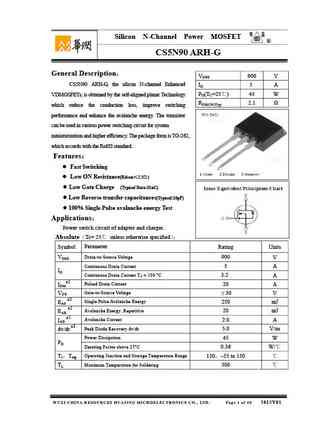
Silicon N-Channel Power MOSFET R CS5N90 ARH-G General Description VDSS 900 V CS5N90 ARH-G, the silicon N-channel Enhanced ID 5 A PD(TC=25 ) 45 W VDMOSFETs, is obtained by the self-aligned planar Technology RDS(ON)Typ 2.1 which reduce the conduction loss, improve switching performance and enhance the avalanche energy. The transistor can be used in various p... See More ⇒
0.32. Size:424K wuxi china
cs5n90fa9h.pdf
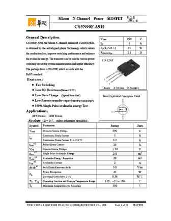
Silicon N-Channel Power MOSFET R CS5N90F A9H General Description VDSS 900 V CS5N90F A9H, the silicon N-channel Enhanced VDMOSFETs, ID 5 A PD(TC=25 ) 45 W is obtained by the self-aligned planar Technology which reduce RDS(ON)Typ 2.1 the conduction loss, improve switching performance and enhance the avalanche energy. The transistor can be used in various power... See More ⇒
0.33. Size:1118K cn hmsemi
hm5n90.pdf
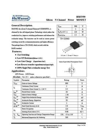
HM5N90 Silicon N-Channel Power MOSFET General Description VDSS 900 V HM5N90, the silicon N-channel Enhanced VDMOSFETs, is ID 5 A PD(TC=25 ) 110 W obtained by the self-aligned planar Technology which reduce the RDS(ON)Typ 2.1 conduction loss, improve switching performance and enhance the avalanche energy. The transistor can be used in various power switching circuit... See More ⇒
0.34. Size:539K cn hmsemi
hm85n90.pdf
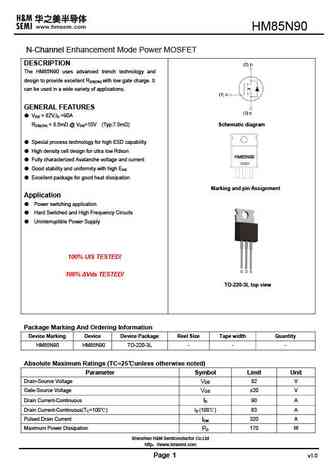
HM85N90 N-Channel Enhancement Mode Power MOSFET DESCRIPTION The HM85N90 uses advanced trench technology and design to provide excellent RDS(ON) with low gate charge. It can be used in a wide variety of applications. GENERAL FEATURES VDS = 82V,ID =90A RDS(ON) ... See More ⇒
0.35. Size:970K cn hmsemi
hms5n90k hms5n90i.pdf
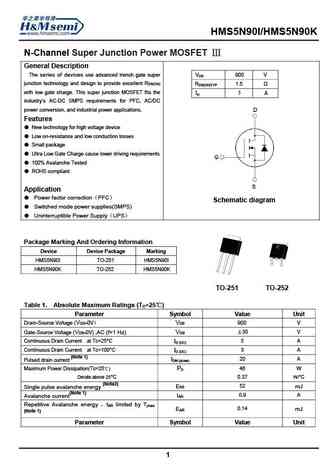
HMS5N90I/HMS5N90K N-Channel Super Junction Power MOSFET General Description The series of devices use advanced trench gate super V 900 V DS junction technology and design to provide excellent RDS(ON) R 1.5 DS(ON)TYP with low gate charge. This super junction MOSFET fits the ID 5 A industry s AC-DC SMPS requirements for PFC, AC/DC power conversion, and industrial powe... See More ⇒
0.36. Size:2708K cn scilicon
sfp055n90c3 sfb052n90c3.pdf
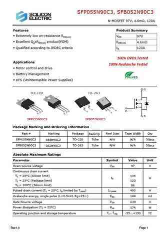
SFP055N90C3, SFB052N90C3 N-MOSFET 97V, 4.6m , 120A Features Product Summary Extremely low on-resistance RDS(on) VDS 97V Excellent QgxRDS(on) product(FOM) RDS(on) 4.6m Qualified according to JEDEC criteria ID 120A 100% DVDS Tested Applications 100% Avalanche Tested Motor control and drive 100% Avalanche Tested 100% Avalanche Tested Battery management ... See More ⇒
Detailed specifications: 11N90, 12N90, 9N95, 9N100, 1N90, 2N90, 3N90, 4N90, 2N7000, 6N90, 7N90, 1N80, 2N80, 3N80, 4N80, 5N80, 6N80
Keywords - 5N90 MOSFET specs
5N90 cross reference
5N90 equivalent finder
5N90 pdf lookup
5N90 substitution
5N90 replacement
Can't find your MOSFET?
Learn how to find a substitute transistor by analyzing voltage, current and package compatibility