5N40 Specs and Replacement
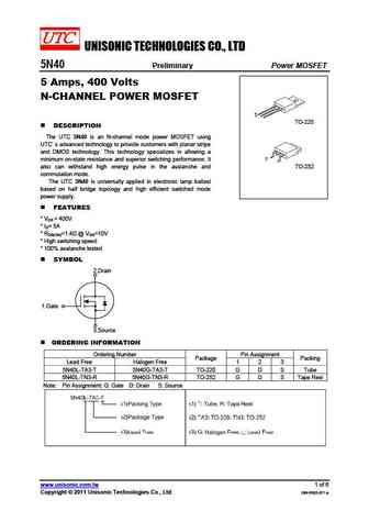
Type Designator: 5N40
Type of Transistor: MOSFET
Type of Control Channel: N-Channel
Absolute Maximum Ratings
Pd ⓘ - Maximum Power Dissipation: 69 W
|Vds|ⓘ - Maximum Drain-Source Voltage: 400 V
|Vgs|ⓘ - Maximum Gate-Source Voltage: 30 V
|Id| ⓘ - Maximum Drain Current: 5 A
Tj ⓘ - Maximum Junction Temperature: 150 °C
Electrical Characteristics
tr ⓘ - Rise Time: 46 nS
Cossⓘ - Output Capacitance: 80 pF
RDSonⓘ - Maximum Drain-Source On-State Resistance: 0.96 Ohm
5N40 substitution
- MOSFET ⓘ Cross-Reference Search
5N40 datasheet
5n40.pdf
UNISONIC TECHNOLOGIES CO., LTD 5N40 Preliminary Power MOSFET 5 Amps, 400 Volts N-CHANNEL POWER MOSFET 1 TO-220 DESCRIPTION The UTC 5N40 is an N-channel mode power MOSFET using UTC s advanced technology to provide customers with planar stripe and DMOS technology. This technology specializes in allowing a 1 minimum on-state resistance and superior switching performance. It ... See More ⇒
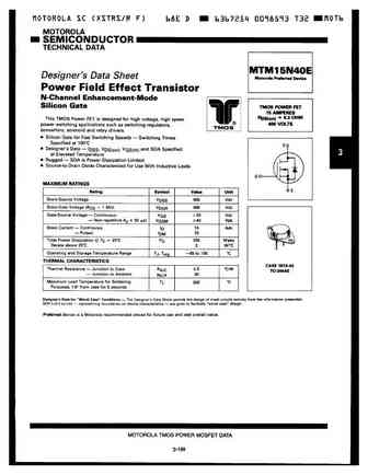
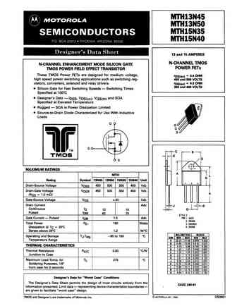
ixth12n45ma ixth12n45mb ixth12n50ma ixth12n50mb ixth15n35ma ixth15n35mb ixth15n40ma ixth15n40mb ixtz42n20mb ixtz67n10ma ixtz67n10mb.pdf
... See More ⇒
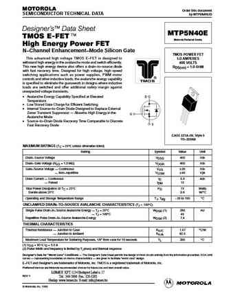
mtp5n40e.pdf
MOTOROLA Order this document SEMICONDUCTOR TECHNICAL DATA by MTP5N40E/D Designer's Data Sheet MTP5N40E TMOS E-FET. Motorola Preferred Device High Energy Power FET N Channel Enhancement Mode Silicon Gate TMOS POWER FET This advanced high voltage TMOS E FET is designed to 5.0 AMPERES withstand high energy in the avalanche mode and switch efficiently. 400 VOLTS This new ... See More ⇒
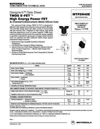
mtp5n40erev1a.pdf
MOTOROLA Order this document SEMICONDUCTOR TECHNICAL DATA by MTP5N40E/D Designer's Data Sheet MTP5N40E TMOS E-FET. Motorola Preferred Device High Energy Power FET N Channel Enhancement Mode Silicon Gate TMOS POWER FET This advanced high voltage TMOS E FET is designed to 5.0 AMPERES withstand high energy in the avalanche mode and switch efficiently. 400 VOLTS This new ... See More ⇒
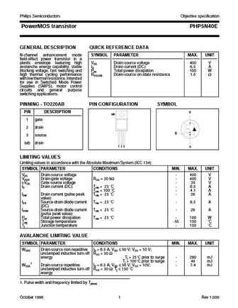
php5n40e 1.pdf
Philips Semiconductors Objective specification PowerMOS transistor PHP5N40E GENERAL DESCRIPTION QUICK REFERENCE DATA N-channel enhancement mode SYMBOL PARAMETER MAX. UNIT field-effect power transistor in a plastic envelope featuring high VDS Drain-source voltage 400 V avalanche energy capability, stable ID Drain current (DC) 6.5 A blocking voltage, fast switching and Ptot Total power d... See More ⇒
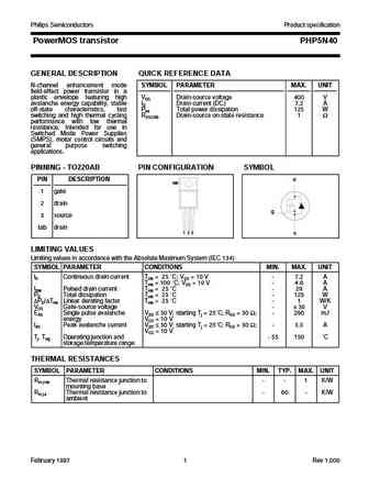
php5n40 1.pdf
Philips Semiconductors Product specification PowerMOS transistor PHP5N40 GENERAL DESCRIPTION QUICK REFERENCE DATA N-channel enhancement mode SYMBOL PARAMETER MAX. UNIT field-effect power transistor in a plastic envelope featuring high VDS Drain-source voltage 400 V avalanche energy capability, stable ID Drain current (DC) 7.2 A off-state characteristics, fast Ptot Total power dissipati... See More ⇒
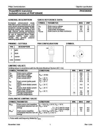
phx5n40e 1.pdf
Philips Semiconductors Objective specification PowerMOS transistor PHX5N40E Isolated version of PHP10N40E GENERAL DESCRIPTION QUICK REFERENCE DATA N-channel enhancement mode SYMBOL PARAMETER MAX. UNIT field-effect power transistor in a full pack, plastic envelope featuring high VDS Drain-source voltage 400 V avalanche energy capability, stable ID Drain current (DC) 4.9 A blocking vol... See More ⇒
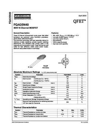
fqa35n40.pdf
April 2000 TM QFET QFET QFET QFET 400V N-ChanneI MOSFET GeneraI Description Features These N-Channel enhancement mode power field effect 35A, 400V, RDS(on) = 0.105 @VGS = 10 V transistors are produced using Fairchild s proprietary, Low gate charge ( typical 110 nC) planar stripe, DMOS technology. Low Crss ( typical 65 pF) This advanced technology has bee... See More ⇒
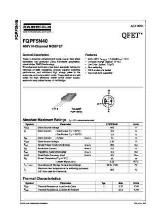
fqpf5n40.pdf
April 2000 TM QFET QFET QFET QFET 400V N-ChanneI MOSFET GeneraI Description Features These N-Channel enhancement mode power field effect 3.0A, 400V, RDS(on) = 1.6 @VGS = 10 V transistors are produced using Fairchild s proprietary, Low gate charge ( typical 10 nC) planar stripe, DMOS technology. Low Crss ( typical 7.0 pF) This advanced technology has been... See More ⇒
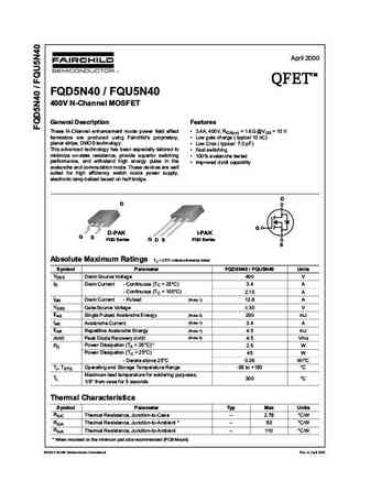
fqd5n40tf fqd5n40tm fqu5n40tu.pdf
April 2000 TM QFET QFET QFET QFET FQD5N40 / FQU5N40 400V N-ChanneI MOSFET GeneraI Description Features These N-Channel enhancement mode power field effect 3.4A, 400V, RDS(on) = 1.6 @VGS = 10 V transistors are produced using Fairchild s proprietary, Low gate charge ( typical 10 nC) planar stripe, DMOS technology. Low Crss ( typical 7.0 pF) This advanced technology ... See More ⇒
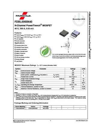
fdbl0065n40.pdf
November 2014 FDBL0065N40 N-Channel PowerTrench MOSFET 40 V, 300 A, 0.65 m Features Typical RDS(on) = 0.5 m at VGS = 10V, ID = 80 A Typical Qg(tot) = 220 nC at VGS = 10V, ID = 80 A UIS Capability D RoHS Compliant Applications Industrial Motor Drive G Industrial Power Supply Industrial Automation Battery Operated tools S Battery Protection For current package... See More ⇒
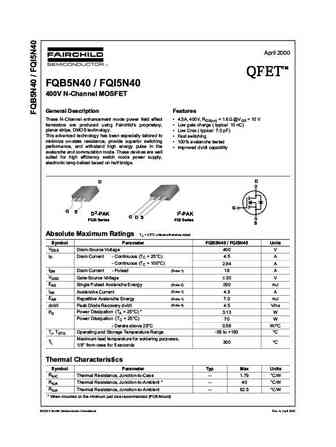
fqb5n40tm fqi5n40tu.pdf
April 2000 TM QFET QFET QFET QFET FQB5N40 / FQI5N40 400V N-ChanneI MOSFET GeneraI Description Features These N-Channel enhancement mode power field effect 4.5A, 400V, RDS(on) = 1.6 @VGS = 10 V transistors are produced using Fairchild s proprietary, Low gate charge ( typical 10 nC) planar stripe, DMOS technology. Low Crss ( typical 7.0 pF) This advanced technology... See More ⇒
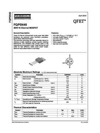
fqp5n40.pdf
April 2000 TM QFET QFET QFET QFET 400V N-ChanneI MOSFET GeneraI Description Features These N-Channel enhancement mode power field effect 4.5A, 400V, RDS(on) = 1.6 @VGS = 10 V transistors are produced using Fairchild s proprietary, Low gate charge ( typical 10 nC) planar stripe, DMOS technology. Low Crss ( typical 7.0 pF) This advanced technology has been ... See More ⇒
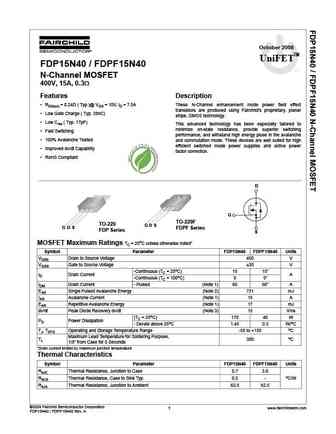
fdp15n40 fdpf15n40.pdf
October 2008 UniFETTM FDP15N40 / FDPF15N40 tm N-Channel MOSFET 400V, 15A, 0.3 Features Description RDS(on) = 0.24 ( Typ.)@ VGS = 10V, ID = 7.5A These N-Channel enhancement mode power field effect transistors are produced using Fairchild s proprietary, planar Low Gate Charge ( Typ. 28nC) stripe, DMOS technology. Low Crss ( Typ. 17pF) This advanced technology has ... See More ⇒
fqu5n40 fqd5n40.pdf
April 2000 TM QFET QFET QFET QFET FQD5N40 / FQU5N40 400V N-ChanneI MOSFET GeneraI Description Features These N-Channel enhancement mode power field effect 3.4A, 400V, RDS(on) = 1.6 @VGS = 10 V transistors are produced using Fairchild s proprietary, Low gate charge ( typical 10 nC) planar stripe, DMOS technology. Low Crss ( typical 7.0 pF) This advanced technology ... See More ⇒
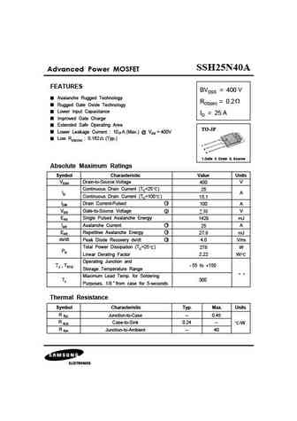
ssh25n40a.pdf
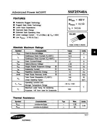
SSH25N40A Advanced Power MOSFET FEATURES BVDSS = 400 V Avalanche Rugged Technology RDS(on) = 0.2 Rugged Gate Oxide Technology Lower Input Capacitance ID = 25 A Improved Gate Charge Extended Safe Operating Area TO-3P Lower Leakage Current 10 A (Max.) @ VDS = 400V Low RDS(ON) 0.162 (Typ.) 1 2 3 1.Gate 2. Drain 3. Source Absolute Maximum Ratings Symbol C... See More ⇒
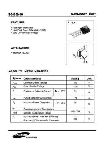
sgi25n40.pdf
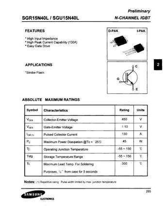
N-CHANNEL IGBT SGI25N40 FEATURES I2 - PAK * High Input Impedance * High Peak Current Capability(170A) * Easy Drive by Gate Voltage C APPLICATIONS * STROBE FLASH G E ABSOLUTE MAXIMUM RATINGS Symbol Characteristics Unit Rating VCES Collector-Emitter Voltage V 400 VGE Gate - Emitter Voltage V 25 IC Continuous Collector Current Tc = 25 25 A ICM Pulsed Collector Curren... See More ⇒
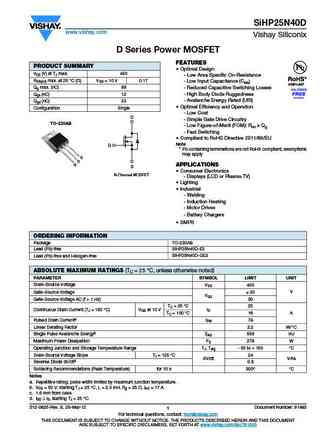
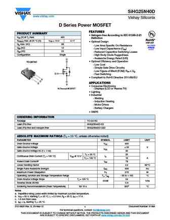
sihg25n40d.pdf
SiHG25N40D www.vishay.com Vishay Siliconix D Series Power MOSFET FEATURES PRODUCT SUMMARY Halogen-free According to IEC 61249-2-21 VDS (V) at TJ max. 450 Definition RDS(on) max. at 25 C ( ) VGS = 10 V 0.17 Optimal Design Qg max. (nC) 88 - Low Area Specific On-Resistance Qgs (nC) 12 - Low Input Capacitance (Ciss) Qgd (nC) 23 - Reduced Capacitive Switching Losses Conf... See More ⇒
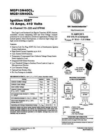
mgp15n40cl mgb15n40cl.pdf
MGP15N40CL, MGB15N40CL Preferred Device Ignition IGBT 15 Amps, 410 Volts N-Channel TO-220 and D2PAK http //onsemi.com This Logic Level Insulated Gate Bipolar Transistor (IGBT) features 15 AMPERES monolithic circuitry integrating ESD and Over-Voltage clamped protection for use in inductive coil drivers applications. Primary uses 410 VOLTS (Clamped) include Ignition, Direct Fuel Injec... See More ⇒
fdb0105n407l.pdf
Is Now Part of To learn more about ON Semiconductor, please visit our website at www.onsemi.com Please note As part of the Fairchild Semiconductor integration, some of the Fairchild orderable part numbers will need to change in order to meet ON Semiconductor s system requirements. Since the ON Semiconductor product management systems do not have the ability to manage part nomenclatur... See More ⇒
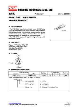
25n40.pdf
UNISONIC TECHNOLOGIES CO., LTD 25N40 Preliminary Power MOSFET 400V, 26A N-CHANNEL POWER MOSFET DESCRIPTION The UTC 25N40 is an N-channel mode power MOSFET using UTC s advanced technology to provide customers with planar stripe and DMOS technology. This technology allows a minimum on-state resistance and superior switching performance. It also can withstand high energy pulse... See More ⇒
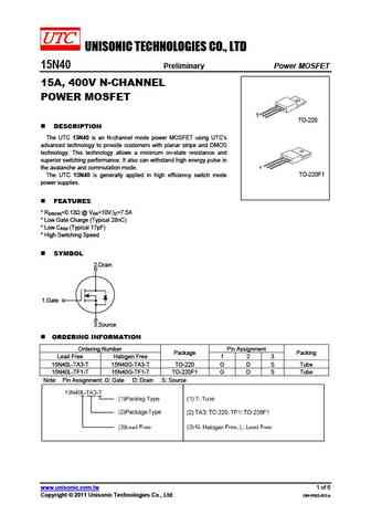
15n40.pdf
UNISONIC TECHNOLOGIES CO., LTD 15N40 Preliminary Power MOSFET 15A, 400V N-CHANNEL POWER MOSFET 1 TO-220 DESCRIPTION The UTC 15N40 is an N-channel mode power MOSFET using UTC s advanced technology to provide customers with planar stripe and DMOS technology. This technology allows a minimum on-state resistance and superior switching performance. It also can withstand high ene... See More ⇒
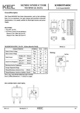
kmb035n40dc.pdf
SEMICONDUCTOR KMB035N40DC TECHNICAL DATA N-Ch Trench MOSFET General Description This Trench MOSFET has better characteristics, such as fast switching time, low on resistance, low gate charge and excellent avalanche A K DIM MILLIMETERS characteristics. It is mainly suitable for Back-light Inverter and power L C D _ A 6.60 + 0.20 _ B 6.10 + 0.20 Supply. _ C 5.34 + 0.30 _ D 0.70 ... See More ⇒
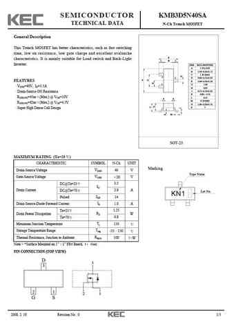
kmb3d5n40sa.pdf
SEMICONDUCTOR KMB3D5N40SA TECHNICAL DATA N-Ch Trench MOSFET General Description This Trench MOSFET has better characteristics, such as fast switching time, low on resistance, low gate charge and excellent avalanche E characteristics. It is mainly suitable for Load switch and Back-Light L B L Inverter. DIM MILLIMETERS _ + A 2.93 0.20 B 1.30+0.20/-0.15 C 1.30 MAX 2 3 D 0.40+0.15/... See More ⇒
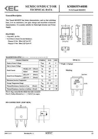
kmb035n40db.pdf
SEMICONDUCTOR KMB035N40DB TECHNICAL DATA N-Ch Trench MOSFET General Description This Trench MOSFET has better characteristics, such as fast switching time, low on resistance, low gate charge and excellent avalanche A characteristics. It is mainly suitable for Back-light Inverter and Power K DIM MILLIMETERS L C D _ A 6.60 + 0.20 Supply. _ B 6.10 + 0.20 _ C 5.34 + 0.30 _ D 0.70 ... See More ⇒
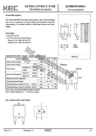
kmb035n40da.pdf
SEMICONDUCTOR KMB035N40DA TECHNICAL DATA N-Ch Trench MOSFET General Description This Trench MOSFET has better characteristics, such as fast switching time, low on resistance, low gate charge and excellent avalanche A K DIM MILLIMETERS L characteristics. It is mainly suitable for Back-light Inverter and Power C D _ A 6.60 + 0.20 _ B 6.10 + 0.20 Supply. _ C 5.34 + 0.30 _ D 0.70 ... See More ⇒
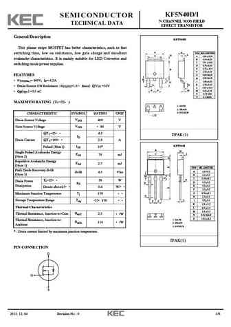
kf5n40d.pdf
KF5N40D/I SEMICONDUCTOR N CHANNEL MOS FIELD TECHNICAL DATA EFFECT TRANSISTOR General Description KF5N40D This planar stripe MOSFET has better characteristics, such as fast A K DIM MILLIMETERS switching time, low on resistance, low gate charge and excellent L C D _ A 6.60 + 0.20 avalanche characteristics. It is mainly suitable for LED Convertor and _ B 6.10 + 0.20 _ C 5.34 +... See More ⇒
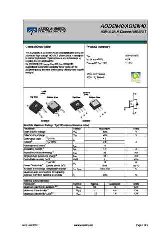
aod5n40.pdf
AOD5N40/AOI5N40 400V,4.2A N-Channel MOSFET General Description Product Summary The AOD5N40 & AOI5N40 have been fabricated using an advanced high voltage MOSFET process that is designed VDS 500V@150 to deliver high levels of performance and robustness in ID (at VGS=10V) 4.2A popular AC-DC applications. RDS(ON) (at VGS=10V) ... See More ⇒
aoi5n40.pdf
AOD5N40/AOI5N40 400V,4.2A N-Channel MOSFET General Description Product Summary The AOD5N40 & AOI5N40 have been fabricated using an advanced high voltage MOSFET process that is designed VDS 500V@150 to deliver high levels of performance and robustness in ID (at VGS=10V) 4.2A popular AC-DC applications. RDS(ON) (at VGS=10V) ... See More ⇒
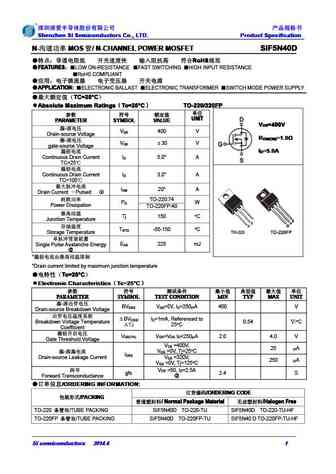
sif5n40d.pdf
Shenzhen SI Semiconductors Co., LTD. Product Specification Shenzhen SI Semiconductors Co., LTD. Product Specification Shenzhen SI Semiconductors Co., LTD. Product Specification Shenzhen SI Semiconductors Co., LTD. Product Specification N- MOS / N-CHANNEL POWER MOSFET SIF5N40D N- MOS / N-CHANNEL POWER MOSFET SIF5N40D N- MOS / N-CHANN... See More ⇒
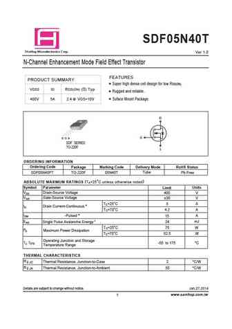
sdf05n40t.pdf
SDF05N40T a S mHop Microelectronics C orp. Ver 1.0 N-Channel Enhancement Mode Field Effect Transistor FEATURES PRODUCT SUMMARY Super high dense cell design for low RDS(ON). VDSS ID RDS(ON) ( ) Typ Rugged and reliable. 400V 5A 2.4 @ VGS=10V Suface Mount Package. D G G D S SDF SERIES TO-220F S ORDERING INFORMATION Ordering Code Package Marking Code Delivery Mode RoHS Status Tu... See More ⇒
mdis5n40th.pdf
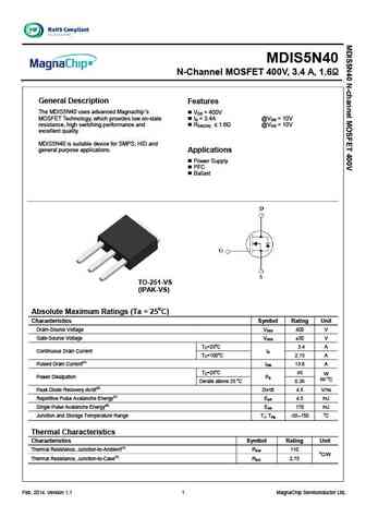
MDIS5N40 N-Channel MOSFET 400V, 3.4 A, 1.6 General Description Features The MDIS5N40 uses advanced Magnachip s V = 400V DS MOSFET Technology, which provides low on-state I = 3.4A @V = 10V D GS resistance, high switching performance and RDS(ON) 1.6 @VGS = 10V excellent quality. MDIS5N40 is suitable device for SMPS, HID and general purpose application... See More ⇒
mdd5n40rh mdi5n40th.pdf
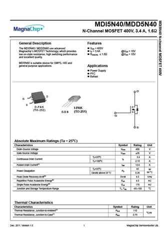
MDI5N40/MDD5N40 N-Channel MOSFET 400V, 3.4 A, 1.6 General Description Features The MDI5N40 / MDD5N40 use advanced VDS = 400V Magnachip s MOSFET Technology, which provides ID = 3.4A @VGS = 10V low on-state resistance, high switching performance @VGS = 10V RDS(ON) 1.6 and excellent quality. MDI5N40 is suitable device for SMPS, HID and general pur... See More ⇒
bl25n40-p bl25n40-a bl25n40-w bl25n40-f.pdf
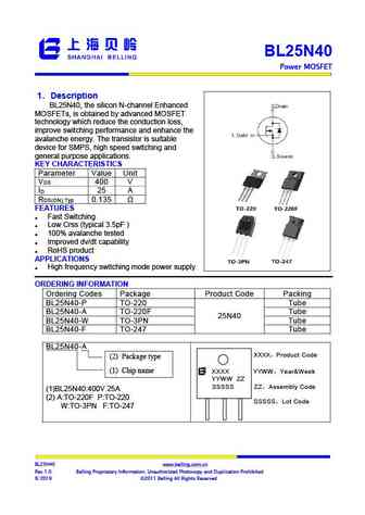
BL25N40 Power MOSFET 1 Description Step-Down Converter BL25N40, the silicon N-channel Enhanced , MOSFETs, is obtained by advanced MOSFET technology which reduce the conduction loss, improve switching performance and enhance the avalanche energy. The transistor is suitable device for SMPS, high speed switching and general purpose applications. KEY CHARACTERISTICS Pa... See More ⇒
hfd5n40.pdf
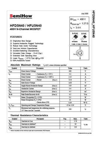
July 2005 BVDSS = 400 V RDS(on) typ HFD5N40 / HFU5N40 ID = 3.4 A 400V N-Channel MOSFET D-PAK I-PAK 2 FEATURES 1 1 3 2 3 Originative New Design HFD5N40 HFU5N40 Superior Avalanche Rugged Technology 1.Gate 2. Drain 3. Source Robust Gate Oxide Technology Very Low Intrinsic Capacitances Excellent Switching Characteristics Unrivalled Gate Charge 13 nC (Typ... See More ⇒
hfd5n40 hfu5n40.pdf
July 2005 BVDSS = 400 V RDS(on) typ HFD5N40 / HFU5N40 ID = 3.4 A 400V N-Channel MOSFET D-PAK I-PAK 2 FEATURES 1 1 3 2 3 Originative New Design HFD5N40 HFU5N40 Superior Avalanche Rugged Technology 1.Gate 2. Drain 3. Source Robust Gate Oxide Technology Very Low Intrinsic Capacitances Excellent Switching Characteristics Unrivalled Gate Charge 13 nC (Typ... See More ⇒
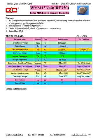
wvm15n40.pdf
Shaanxi Qunli Electric Co., Ltd Add. No. 1 Qunli Road,Baoji City,Shaanxi,China WVM15N40(IRF350) Power MOSFET(N-channel) Transistor Features 1. It s voltage control component with good input impedance, small starting power dissipation, wide area of safe operation, good temperature stability. 2. Implementation of standards QZJ840611 3. Use for high speed switch, circuit of power s... See More ⇒
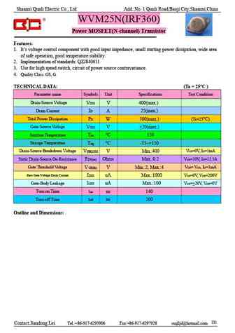
wvm25n40.pdf
Shaanxi Qunli Electric Co., Ltd Add. No. 1 Qunli Road,Baoji City,Shaanxi,China WVM25N(IRF360) Power MOSFET(N-channel) Transistor Features 1. It s voltage control component with good input impedance, small starting power dissipation, wide area of safe operation, good temperature stability. 2. Implementation of standards QZJ840611 3. Use for high speed switch, circuit of power sou... See More ⇒
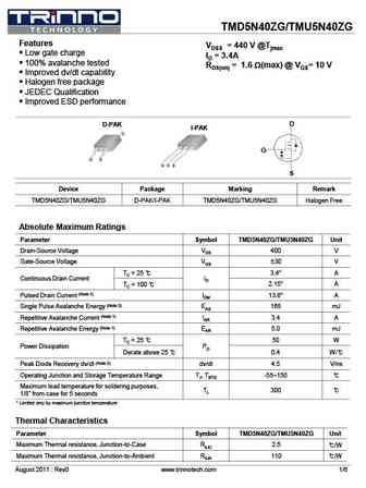
tmd5n40zg tmu5n40zg.pdf
TMD5N40ZG/TMU5N40ZG Features VDSS = 440 V @Tjmax Low gate charge ID = 3.4A 100% avalanche tested RDS(on) = 1.6 W(max) @ VGS= 10 V Improved dv/dt capability Halogen free package JEDEC Qualification Improved ESD performance D-PAK D I-PAK G S Device Package Marking Remark TMD5N40ZG/TMU5N40ZG D-PAK/I-PAK TMD5N40ZG/TMU5N40ZG Halogen Free Abso... See More ⇒
25n40a.pdf
INCHANGE Semiconductor isc N-Channel MOSFET Transistor 25N40A FEATURES Drain Current I = 25A@ T =25 D C Drain Source Voltage V = 400V(Min) DSS Static Drain-Source On-Resistance R = 0.2 (Max) DS(on) Fast Switching 100% avalanche tested Minimum Lot-to-Lot variations for robust device performance and reliable operation. APPLICATIONS Switch mode power suppl... See More ⇒
aod5n40.pdf
isc N-Channel MOSFET Transistor AOD5N40 FEATURES Drain Current I = 4.2A@ T =25 D C Drain Source Voltage- V =400V(Min) DSS Static Drain-Source On-Resistance R =1.6 (Max) DS(on) 100% avalanche tested Minimum Lot-to-Lot variations for robust device performance and reliable operation DESCRIPTION Designed for use in switch mode power supplies and general purpose... See More ⇒
mdi5n40th.pdf
isc N-Channel MOSFET Transistor MDI5N40TH FEATURES Drain Current I = 3.4A@ T =25 D C Drain Source Voltage V = 400V(Min) DSS Static Drain-Source On-Resistance R = 1.6 (Max) @V = 10V DS(on) GS 100% avalanche tested Minimum Lot-to-Lot variations for robust device performance and reliable operation DESCRIPTION motor drive, DC-DC converter, power switch and solen... See More ⇒
mdi5n40rh.pdf
isc N-Channel MOSFET Transistor MDI5N40RH FEATURES Drain Current I = 3.4A@ T =25 D C Drain Source Voltage V = 400V(Min) DSS Static Drain-Source On-Resistance R = 1.6 (Max) @V = 10V DS(on) GS 100% avalanche tested Minimum Lot-to-Lot variations for robust device performance and reliable operation DESCRIPTION motor drive, DC-DC converter, power switch and solen... See More ⇒
mdis5n40th.pdf
isc N-Channel MOSFET Transistor MDIS5N40TH FEATURES Drain Current I = 3.4A@ T =25 D C Drain Source Voltage V = 400V(Min) DSS Static Drain-Source On-Resistance R = 1.6 (Max) @V = 10V DS(on) GS 100% avalanche tested Minimum Lot-to-Lot variations for robust device performance and reliable operation DESCRIPTION motor drive, DC-DC converter, power switch and sole... See More ⇒
aoi5n40.pdf
isc N-Channel MOSFET Transistor AOI5N40 FEATURES Drain Current I = 4.2A@ T =25 D C Drain Source Voltage- V =400V(Min) DSS Static Drain-Source On-Resistance R =1.6 (Max) DS(on) 100% avalanche tested Minimum Lot-to-Lot variations for robust device performance and reliable operation DESCRIPTION Designed for use in switch mode power supplies and general purpose... See More ⇒
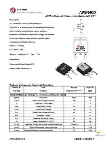
ap5n40d.pdf
AP5N40D 400V N-Channel Enhancement Mode MOSFET Description The AP5N40D is silicon N-channel Enhanced VDMOSFETs, is obtained by the self-aligned planar Technology which reduce the conduction loss, improve switching performance and enhance the avalanche energy. The transistor can be used in various power switching circuit for system miniaturization and higher efficiency. Genera... See More ⇒
Detailed specifications: 5N50K , 6N50 , 7N50 , 8N50 , 1N40 , 2N40 , 3N40 , 4N40 , IRFB3607 , 6N40 , 7N40 , 8N40 , 9N40 , 10N40 , 11N40 , 12N40 , 13N40 .
Keywords - 5N40 MOSFET specs
5N40 cross reference
5N40 equivalent finder
5N40 pdf lookup
5N40 substitution
5N40 replacement
Learn how to find the right MOSFET substitute. A guide to cross-reference, check specs and replace MOSFETs in your circuits.
