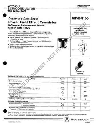
6N10 Specs and Replacement
Type Designator: 6N10
Type of Transistor: MOSFET
Type of Control Channel: N-Channel
Absolute Maximum Ratings
Pd ⓘ - Maximum Power Dissipation: 16 W
|Vds|ⓘ - Maximum Drain-Source Voltage: 100 V
|Vgs|ⓘ - Maximum Gate-Source Voltage: 20 V
|Id| ⓘ - Maximum Drain Current: 6.5 A
Tj ⓘ - Maximum Junction Temperature: 150 °C
Electrical Characteristics
tr ⓘ - Rise Time: 30 nS
Cossⓘ - Output Capacitance: 80 pF
Rds ⓘ - Maximum Drain-Source On-State Resistance: 0.16 Ohm
6N10 substitution
- MOSFET ⓘ Cross-Reference Search
6N10 datasheet
6n10.pdf
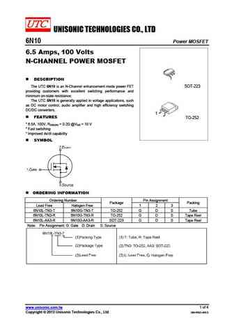
UNISONIC TECHNOLOGIES CO., LTD 6N10 Power MOSFET 6.5 Amps, 100 Volts N-CHANNEL POWER MOSFET 1 DESCRIPTION The UTC 6N10 is an N-Channel enhancement mode power FET SOT-223 providing customers with excellent switching performance and minimum on-state resistance. The UTC 6N10 is generally applied in voltage applications, such as DC motor control, audio amplifier and high effi... See More ⇒
std6n10 std6n10-1 std6n10t4.pdf
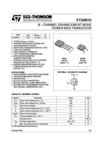
STD6N10 N - CHANNEL ENHANCEMENT MODE POWER MOS TRANSISTOR TYPE VDSS RDS(on) ID STD6N10 100 V ... See More ⇒
ntmfs3d6n10mclt1g.pdf
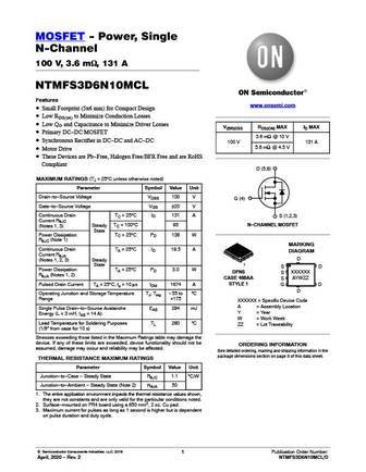
MOSFET - Power, Single N-Channel 100 V, 3.6 mW, 131 A NTMFS3D6N10MCL Features www.onsemi.com Small Footprint (5x6 mm) for Compact Design Low RDS(on) to Minimize Conduction Losses Low QG and Capacitance to Minimize Driver Losses V(BR)DSS RDS(ON) MAX ID MAX Primary DC-DC MOSFET 3.6 mW @ 10 V Synchronous Rectifier in DC-DC and AC-DC 100 V 131 A 5.8 mW @ 4.5 V ... See More ⇒
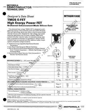
mtv6n100e.pdf
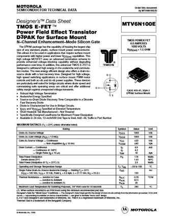
MOTOROLA Order this document SEMICONDUCTOR TECHNICAL DATA by MTV6N100E/D Designer's Data Sheet MTV6N100E TMOS E-FET. Power Field Effect Transistor D3PAK for Surface Mount TMOS POWER FET N Channel Enhancement Mode Silicon Gate 6.0 AMPERES 1000 VOLTS The D3PAK package has the capability of housing the largest chip RDS(on) = 1.5 OHM size of any standard, plastic, surface m... See More ⇒
mtw6n100e.pdf

MOTOROLA Order this document SEMICONDUCTOR TECHNICAL DATA by MTW6N100E/D Designer's Data Sheet MTW6N100E TMOS E-FET. Motorola Preferred Device Power Field Effect Transistor TO-247 With Isolated Mounting Hole TMOS POWER FET N Channel Enhancement Mode Silicon Gate 6.0 AMPERES 1000 VOLTS This high voltage MOSFET uses an advanced termination RDS(on) = 1.5 OHM scheme to prov... See More ⇒
mtw6n100erev3.pdf
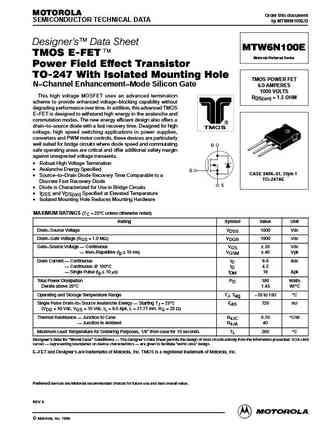
MOTOROLA Order this document SEMICONDUCTOR TECHNICAL DATA by MTW6N100E/D Designer's Data Sheet MTW6N100E TMOS E-FET. Motorola Preferred Device Power Field Effect Transistor TO-247 With Isolated Mounting Hole TMOS POWER FET N Channel Enhancement Mode Silicon Gate 6.0 AMPERES 1000 VOLTS This high voltage MOSFET uses an advanced termination RDS(on) = 1.5 OHM scheme to prov... See More ⇒
mtd6n10e.pdf
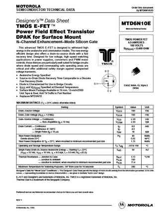
MOTOROLA Order this document SEMICONDUCTOR TECHNICAL DATA by MTD6N10E/D Designer's Data Sheet MTD6N10E TMOS E-FET. Motorola Preferred Device Power Field Effect Transistor DPAK for Surface Mount TMOS POWER FET N Channel Enhancement Mode Silicon Gate 6.0 AMPERES 100 VOLTS This advanced TMOS E FET is designed to withstand high RDS(on) = 0.400 OHM energy in the avalanche... See More ⇒
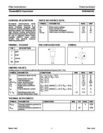
phd6n10e 1.pdf
Philips Semiconductors Product specification PowerMOS transistor PHD6N10E GENERAL DESCRIPTION QUICK REFERENCE DATA N-channel enhancement mode SYMBOL PARAMETER MAX. UNIT field-effect power transistor in a plastic envelope suitable for surface VDS Drain-source voltage 100 V mounting featuring high avalanche ID Drain current (DC) 6.3 A energy capability, stable blocking Ptot Total power d... See More ⇒
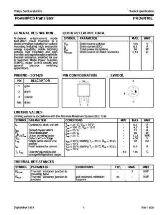
php6n10e 1.pdf
Philips Semiconductors Product specification PowerMOS transistor PHP6N10E GENERAL DESCRIPTION QUICK REFERENCE DATA N-channel enhancement mode SYMBOL PARAMETER MAX. UNIT field-effect power transistor in a plastic envelope featuring high VDS Drain-source voltage 100 V avalanche energy capability, stable ID Drain current (DC) 6.3 A blocking voltage, fast switching and Ptot Total power dis... See More ⇒
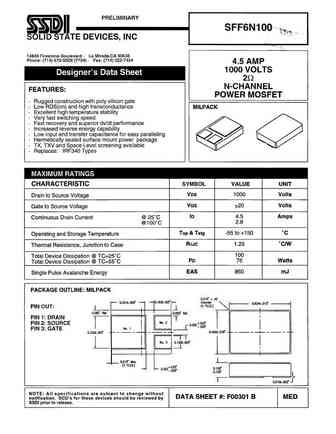
sth6n100.pdf
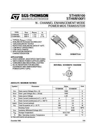
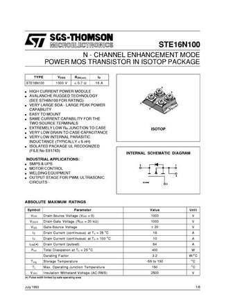
STH6N100 STH6N100FI N - CHANNEL ENHANCEMENT MODE POWER MOS TRANSISTOR TYPE VDSS RDS(on) ID STH6N100 1000 V ... See More ⇒
stp16n10l.pdf
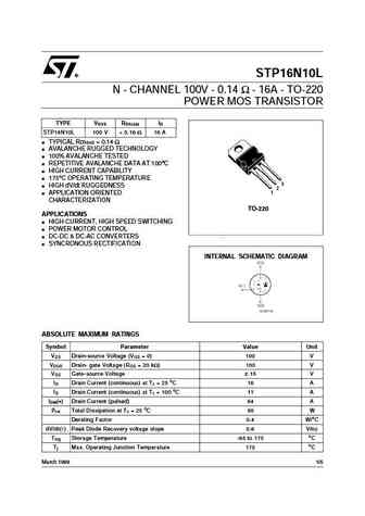
STP16N10L N - CHANNEL 100V - 0.14 - 16A - TO-220 POWER MOS TRANSISTOR TYPE VDSS RDS(on) ID STP16N10L 100 V ... See More ⇒
std6n10.pdf
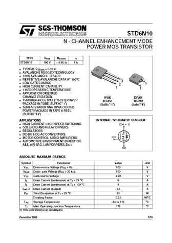
STD6N10 N - CHANNEL ENHANCEMENT MODE POWER MOS TRANSISTOR TYPE VDSS RDS(on) ID STD6N10 100 V ... See More ⇒
np36n10sde.pdf
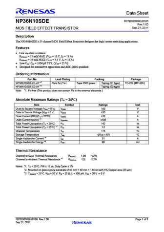
Preliminary Data Sheet R07DS0508EJ0100 NP36N10SDE Rev.1.00 Sep 21, 2011 MOS FIELD EFFECT TRANSISTOR Description The NP36N10SDE is N-channel MOS Field Effect Transistor designed for high current switching applications. Features Low on-state resistance RDS(on)1 = 33 m MAX. (VGS = 10 V, ID = 18 A) RDS(on)2 = 39 m MAX. (VGS = 4.5 V, ID = 18 A) Low Ciss Ciss = 3500... See More ⇒
fdp036n10a.pdf
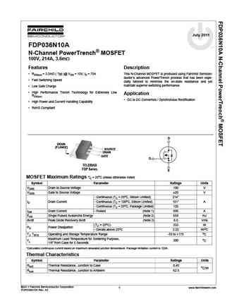
July 2011 FDP036N10A tm N-Channel PowerTrench MOSFET 100V, 214A, 3.6m Features Description RDS(on) = 3.2m ( Typ.)@ VGS = 10V, ID = 75A This N-Channel MOSFET is produced using Fairchild Semicon- ductor s advanced PowerTrench process that has been espe- Fast Switching Speed cially tailored to minimize the on-state resistance and yet maintain superior switching performa... See More ⇒
suu06n10.pdf
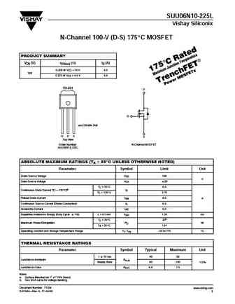
SUU06N10-225L Vishay Siliconix N-Channel 100-V (D-S) 175_CMOSFET PRODUCT SUMMARY VDS (V) rDS(on) ( ) ID (A) 0.200 @ VGS =10V 6.5 100 100 0.225 @ VGS =4.5V 6.0 TO-251 D G and DRAIN-TAB G D S S Top View Order Number N-Channel MOSFET SUU06N10-225L ABSOLUTE MAXIMUM RATINGS (TA = 25_C UNLESS OTHERWISE NOTED) Parameter Symbol Limit Unit Drain-Source Voltage VDS 100 V V Gate-... See More ⇒
sud06n10-225l.pdf
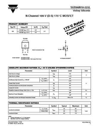
SUD06N10-225L Vishay Siliconix N-Channel 100-V (D-S) 175_C MOSFET PRODUCT SUMMARY VDS (V) rDS(on) (W) ID (A) Qg (Typ) 0.200 @ VGS = 10 V 6.5 100 27 100 2.7 0.225 @ VGS = 4.5 V 6.0 TO-252 D G Drain Connected to Tab G D S Top View S Order Number SUD06N10-225L N-Channel MOSFET SUD06N10-225L E3 (lLead (Pb)-Free) ABSOLUTE MAXIMUM RATINGS (TA = 25_C UNLESS OTHERWISE NOTED) Para... See More ⇒
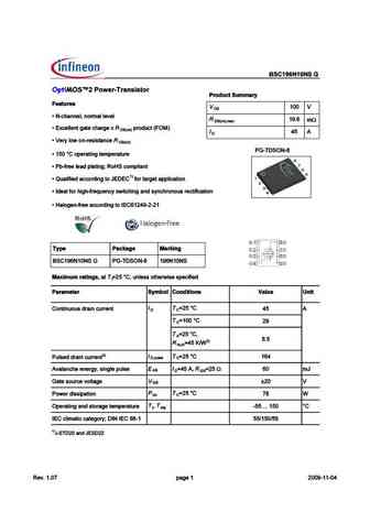
bsc096n10ls5.pdf
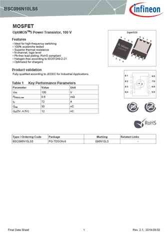
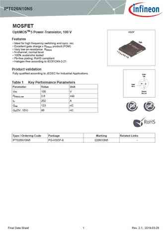
BSC096N10LS5 MOSFET SuperSO8 OptiMOSTM5 Power-Transistor, 100 V 5 8 6 7 Features 7 6 8 5 Ideal for high-frequency switching 100% avalanche tested Superior thermal resistance N-channel, logic level 4 Pb-free lead plating; RoHS compliant 1 3 2 2 Halogen-free according to IEC61249-2-21 3 1 4 Optimized for chargers Product validation Fully quali... See More ⇒
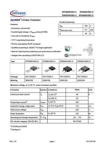
ipp086n10n3g ipi086n10n3g ipb083n10n3g ipd082n10n3g.pdf

IPP086N10N3 G IPI086N10N3 G IPB083N10N3 G IPD082N10N3 G OptiMOS 3 Power-Transistor Product Summary Features VDS 100 V N-channel, normal level RDS(on),max (TO 252) 8.2 mW Excellent gate charge x R product (FOM) DS(on) ID 80 A Very low on-resistance R DS(on) 175 C operating temperature Pb-free lead plating; RoHS compliant Qualified according to JED... See More ⇒
bsb056n10nn3g.pdf
n-Channel Power MOSFET OptiMOS BSB056N10NN3 G Data Sheet 2.5, 2011-05-27 Final Industrial & Multimarket OptiMOS Power-MOSFET BSB056N10NN3 G 1 Description OptiMOS 100V products are class leading power MOSFETs for highest power density and energy efficient solutions. Ultra low gate- and output charges together with lowest on state resistance in small footprint packages make... See More ⇒
ipp126n10n3g ipb123n10n3g ipi126n10n3g.pdf
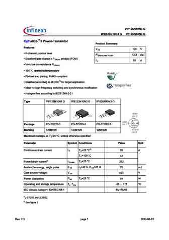
## ! ! # ! ! # ! ! TM # A0... See More ⇒
bsc046n10ns3g.pdf
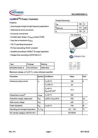
BSC046N10NS3 G OptiMOSTM3 Power-Transistor Product Summary Features VDS 100 V Very low gate charge for high frequency applications RDS(on),max 4.6 mW Optimized for dc-dc conversion ID 100 A N-channel, normal level PG-TDSON-8 Excellent gate charge x R product (FOM) DS(on) Very low on-resistance R DS(on) 150 C operating temperature Pb-free lead plati... See More ⇒
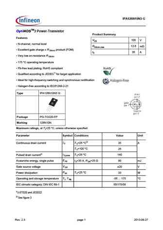
ipa126n10nm3s.pdf
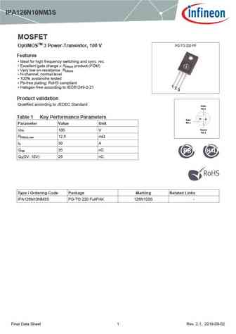
IPA126N10NM3S MOSFET PG-TO 220 FP OptiMOSTM 3 Power-Transistor, 100 V Features Ideal for high frequency switching and sync. rec. Excellent gate charge x R product (FOM) DS(on) Very low on-resistance R DS(on) N-channel, normal level 100% avalanche tested Pb-free plating; RoHS compliant Halogen-free according to IEC61249-2-21 Product validation Qualified... See More ⇒
bsc146n10ls5.pdf
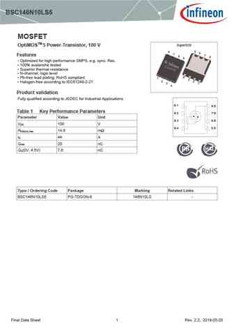
BSC146N10LS5 MOSFET SuperSO8 OptiMOSTM 5 Power-Transistor, 100 V 5 8 6 7 Features 7 6 8 5 Optimized for high performance SMPS, e.g. sync. Rec. 100% avalanche tested Superior thermal resistance N-channel, logic level 4 Pb-free lead plating; RoHS compliant 1 3 2 2 Halogen-free according to IEC61249-2-21 3 1 4 Product validation Fully qualified acco... See More ⇒
bsz146n10ls5.pdf
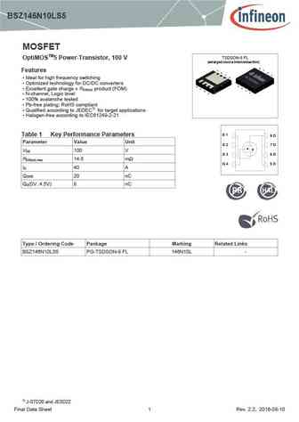
BSZ146N10LS5 MOSFET TSDSON-8 FL OptiMOSTM5 Power-Transistor, 100 V (enlarged source interconnection) Features Ideal for high frequency switching Optimized technology for DC/DC converters Excellent gate charge x R product (FOM) DS(on) N-channel, Logic level 100% avalanche tested Pb-free plating; RoHS compliant Qualified according to JEDEC1) for target app... See More ⇒
ipa086n10n3g.pdf
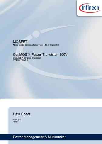
MOSFET Metal Oxide Semiconductor Field Effect Transistor OptiMOS Power-Transistor, 100V OptiMOS 3 Power-Transistor IPA086N10N3 G Data Sheet Rev. 2.4 Final Power Management & Multimarket IPA086N10N3 G OptiMOSTM3 Power-Transistor Product Summary Features VDS 100 V N-channel, normal level RDS(on),max 8.6 mW Excellent gate charge x R product (FOM) DS(on) ID 45 A... See More ⇒
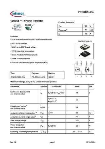
ipg16n10s4l-61a.pdf
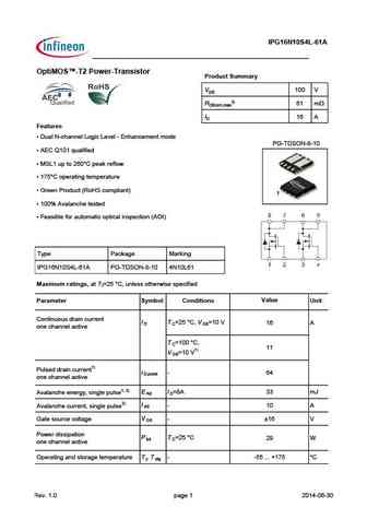
IPG16N10S4L-61A OptiMOS -T2 Power-Transistor Product Summary VDS 100 V RDS(on),max3) 61 mW ID 16 A Features Dual N-channel Logic Level - Enhancement mode PG-TDSON-8-10 AEC Q101 qualified MSL1 up to 260 C peak reflow 175 C operating temperature Green Product (RoHS compliant) 100% Avalanche tested Feasible for automatic optical inspection (AOI) Type... See More ⇒
ipg16n10s4-61a.pdf
IPG16N10S4-61A OptiMOS -T2 Power-Transistor Product Summary VDS 100 V RDS(on),max3) 61 m ID 16 A Features Dual N-channel Normal Level - Enhancement mode PG-TDSON-8-10 AEC Q101 qualified MSL1 up to 260 C peak reflow 175 C operating temperature Green Product (RoHS compliant) 100% Avalanche tested Feasible for automatic optical inspection (AOI) Typ... See More ⇒
ipp086n10n3-g ipi086n10n3-g ipb083n10n3-g ipd082n10n3-g.pdf
IPP086N10N3 G IPI086N10N3 G IPB083N10N3 G IPD082N10N3 G OptiMOS 3 Power-Transistor Product Summary Features VDS 100 V N-channel, normal level RDS(on),max (TO 252) 8.2 mW Excellent gate charge x R product (FOM) DS(on) ID 80 A Very low on-resistance R DS(on) 175 C operating temperature Pb-free lead plating; RoHS compliant Qualified according to JED... See More ⇒
ipa126n10n3g.pdf
IPA126N10N3 G OptiMOSTM3 Power-Transistor Product Summary Features VDS 100 V N-channel, normal level RDS(on),max 12.6 mW Excellent gate charge x R product (FOM) DS(on) ID 35 A Very low on-resistance R DS(on) 175 C operating temperature Pb-free lead plating; RoHS compliant Qualified according to JEDEC1) for target application Ideal for high-freq... See More ⇒
ipt026n10n5.pdf
IPT026N10N5 MOSFET HSOF OptiMOSTM 5 Power-Transistor, 100 V Features Tab Ideal for high frequency switching and sync. rec. Excellent gate charge x R product (FOM) DS(on) Very low on-resistance R DS(on) 1 N-channel, normal level 2 3 4 5 100% avalanche tested 6 7 8 Pb-free plating; RoHS compliant Halogen-free according to IEC61249-2-21 Product val... See More ⇒
ipb123n10n3 ipi126n10n3g ipp126n10n3g.pdf

## ! ! # ! ! # ! ! TM # A0... See More ⇒
ixfh6n100q ixft6n100q.pdf
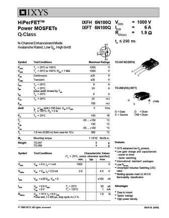
VDSS = 1000 V IXFH 6N100Q HiPerFETTM ID25 = 6 A IXFT 6N100Q Power MOSFETs RDS(on) = 1.9 Q-Class trr 250 ns N-Channel Enhancement Mode Avalanche Rated, Low Qg, High dv/dt Symbol Test Conditions Maximum Ratings TO-247 AD (IXFH) VDSS TJ = 25 C to 150 C 1000 V VDGR TJ = 25 C to 150 C; RGS = 1 M 1000 V VGS Continuous 20 V VG... See More ⇒
ixth16n10d2 ixtt16n10d2.pdf
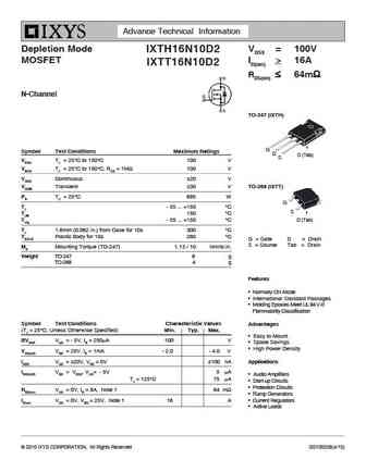
Advance Technical Information Depletion Mode VDSX = 100V IXTH16N10D2 MOSFET ID(on) > 16A IXTT16N10D2 RDS(on) 64m N-Channel TO-247 (IXTH) G Symbol Test Conditions Maximum Ratings D D (Tab) S VDSX TJ = 25 C to 150 C 100 V VDGX TJ = 25 C to 150 C, RGS = 1M 100 V VGSX Continuous 20 V VGSM Transient 30 V TO-268 (IXTT) PD TC = 25 C 695... See More ⇒
ixfn36n100.pdf
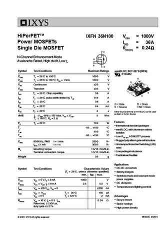
HiPerFETTM IXFN 36N100 V = 1000V DSS Power MOSFETs ID25 = 36A Single Die MOSFET RDS(on) = 0.24 D N-Channel Enhancement Mode G Avalanche Rated, High dv/dt, Low t rr S S Symbol Test Conditions Maximum Ratings miniBLOC, SOT-227 B (IXFN) E153432 VDSS TJ = 25 C to 150 C 1000 V S VDGR TJ = 25 C to 150 C; RGS = 1 M 1000 V G VGS Continuous 20 V VGSM ... See More ⇒
ixfh6n90 ixfh6n100 ixfm6n90 ixfm6n100.pdf
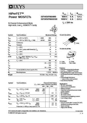
VDSS ID25 RDS(on) HiPerFETTM IXFH/IXFM 6 N90 900 V 6 A 1.8 W Power MOSFETs IXFH/IXFM 6 N100 1000 V 6 A 2.0 W trr 250 ns N-Channel Enhancement Mode High dv/dt, Low trr, HDMOSTM Family Symbol Test Conditions Maximum Ratings TO-247 AD (IXFH) VDSS TJ = 25 C to 150 C 6N90 900 V VDGR TJ = 25 C to 150 C; RGS = 1 MW 6N100 1000 V VGS Continuous 20 V (TAB) VGSM Transient 30 V ID2... See More ⇒
ixta6n100d2-ixtp6n100d2-ixth6n100d2.pdf
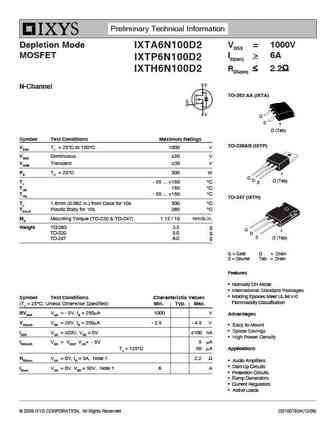
Preliminary Technical Information Depletion Mode VDSX = 1000V IXTA6N100D2 MOSFET ID(on) > 6A IXTP6N100D2 RDS(on) 2.2 IXTH6N100D2 N-Channel TO-263 AA (IXTA) G S D (Tab) Symbol Test Conditions Maximum Ratings TO-220AB (IXTP) VDSX TJ = 25 C to 150 C 1000 V VGSX Continuous 20 V VGSM Transient 30 V PD TC = 25 C 300 W G D D (Tab) TJ - ... See More ⇒
fdp036n10a.pdf

Is Now Part of To learn more about ON Semiconductor, please visit our website at www.onsemi.com Please note As part of the Fairchild Semiconductor integration, some of the Fairchild orderable part numbers will need to change in order to meet ON Semiconductor s system requirements. Since the ON Semiconductor product management systems do not have the ability to manage part nomenclatur... See More ⇒
ntmfs3d6n10mcl.pdf

MOSFET - Power, Single N-Channel 100 V, 3.6 mW, 131 A NTMFS3D6N10MCL Features www.onsemi.com Small Footprint (5x6 mm) for Compact Design Low RDS(on) to Minimize Conduction Losses Low QG and Capacitance to Minimize Driver Losses V(BR)DSS RDS(ON) MAX ID MAX Primary DC-DC MOSFET 3.6 mW @ 10 V Synchronous Rectifier in DC-DC and AC-DC 100 V 131 A 5.8 mW @ 4.5 V ... See More ⇒
nvmfs3d6n10mcl.pdf
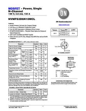
MOSFET - Power, Single N-Channel 100 V, 3.6 mW, 132 A NVMFS3D6N10MCL Features www.onsemi.com Small Footprint (5x6 mm) for Compact Design Low RDS(on) to Minimize Conduction Losses Low QG and Capacitance to Minimize Driver Losses V(BR)DSS RDS(ON) MAX ID MAX NVMFWS3D6N10MCL - Wettable Flank Option for Enhanced 3.6 mW @ 10 V Optical Inspection 100 V 132 A 5.8 mW @ 4.5 ... See More ⇒
utt6n10.pdf
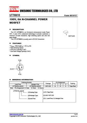
UNISONIC TECHNOLOGIES CO., LTD UTT6N10 Power MOSFET 100V, 6A N-CHANNEL POWER MOSFET DESCRIPTION The UTC UTT6N10 is an N-channel enhancement mode Power FET, it uses UTC s advanced technology to provide customers a 1 minimum on-state resistance, high switching speed and ultra low SOT-223 gate charge. The UTC UTT6N10 is usually used in DC-DC Conversion. FEATURES ... See More ⇒
utt36n10.pdf
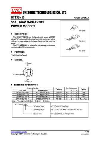
UNISONIC TECHNOLOGIES CO., LTD UTT36N10 Power MOSFET 36A, 100V N-CHANNEL POWER MOSFET DESCRIPTION The UTC UTT36N10 is a N-channel mode power MOSFET using UTC s advanced technology to provide customers with a minimum on-state resistance, low gate charge and high switching speed. The UTC UTT36N10 is suitable for high voltage synchronous rectifier and DC/DC converters, et... See More ⇒
ku086n10p f.pdf
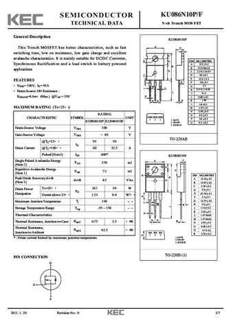
KU086N10P/F SEMICONDUCTOR N-ch Trench MOS FET TECHNICAL DATA General Description KU086N10P A This Trench MOSFET has better characteristics, such as fast O C switching time, low on resistance, low gate charge and excellent F avalanche characteristics. It is mainly suitable for DC/DC Converter, E DIM MILLIMETERS G _ Synchronous Rectification and a load switch in battery powered + ... See More ⇒
cep16n10l ceb16n10l.pdf
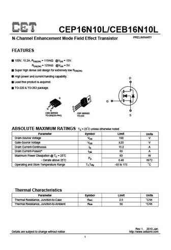
CEP16N10L/CEB16N10L PRELIMINARY N-Channel Enhancement Mode Field Effect Transistor FEATURES 100V, 15.2A, RDS(ON) = 115m @VGS = 10V. RDS(ON) = 125m @VGS = 5V. Super high dense cell design for extremely low RDS(ON). High power and current handing capability. D Lead free product is acquired. TO-220 & TO-263 package. G CEB SERIES CEP SERIES TO-263(DD-PAK) S TO-220 ABSOLUTE MA... See More ⇒
ceu16n10 ced16n10.pdf
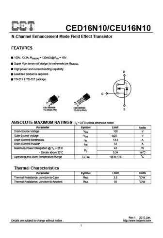
CED16N10/CEU16N10 N-Channel Enhancement Mode Field Effect Transistor FEATURES 100V, 13.3A, RDS(ON) = 120m @VGS = 10V. Super high dense cell design for extremely low RDS(ON). High power and current handing capability. D Lead free product is acquired. TO-251 & TO-252 package. G D G S CEU SERIES CED SERIES S TO-252(D-PAK) TO-251(I-PAK) ABSOLUTE MAXIMUM RATINGS Tc = 25 C unless... See More ⇒
ceu16n10l ced16n10l.pdf
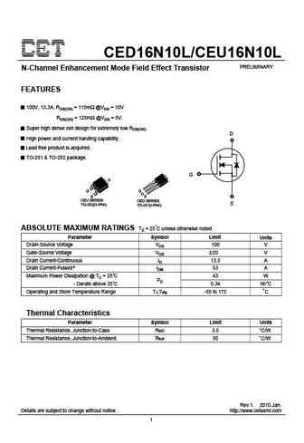
CED16N10L/CEU16N10L PRELIMINARY N-Channel Enhancement Mode Field Effect Transistor FEATURES 100V, 13.3A, RDS(ON) = 115m @VGS = 10V. RDS(ON) = 125m @VGS = 5V. Super high dense cell design for extremely low RDS(ON). D High power and current handing capability. Lead free product is acquired. TO-251 & TO-252 package. G D G S CEU SERIES CED SERIES S TO-252(D-PAK) TO-251(I-P... See More ⇒
cep16n10 ceb16n10.pdf
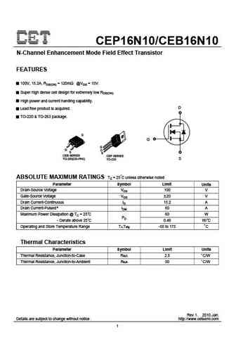
CEP16N10/CEB16N10 N-Channel Enhancement Mode Field Effect Transistor FEATURES 100V, 15.2A, RDS(ON) = 120m @VGS = 10V. Super high dense cell design for extremely low RDS(ON). High power and current handing capability. D Lead free product is acquired. TO-220 & TO-263 package. G CEB SERIES CEP SERIES TO-263(DD-PAK) S TO-220 ABSOLUTE MAXIMUM RATINGS Tc = 25 C unless otherwise noted... See More ⇒
sff116n10m sff116n10z.pdf
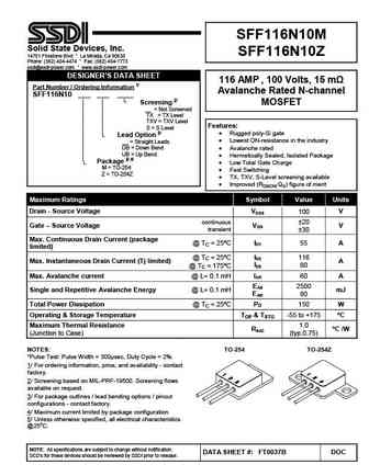
SFF116N10M Solid State Devices, Inc. SFF116N10Z 14701 Firestone Blvd * La Mirada, Ca 90638 Phone (562) 404-4474 * Fax (562) 404-1773 ssdi@ssdi-power.com * www.ssdi-power.com DESIGNER S DATA SHEET 116 AMP , 100 Volts, 15 m Part Number / Ordering Information 1/ Avalanche Rated N-channel SFF116N10 ___ ___ ____ Screening 2/ MOSFET __ = Not Scre... See More ⇒
ap6n100h.pdf
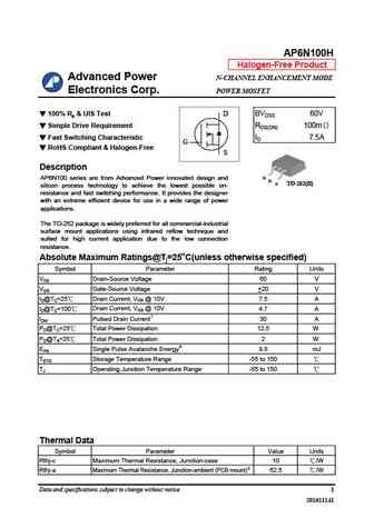
AP6N100H Halogen-Free Product Advanced Power N-CHANNEL ENHANCEMENT MODE Electronics Corp. POWER MOSFET 100% Rg & UIS Test D BVDSS 60V Simple Drive Requirement RDS(ON) 100m Fast Switching Characteristic ID 7.5A G RoHS Compliant & Halogen-Free S Description G AP6N100 series are from Advanced Power innovated design and D S TO-252(H) silicon process technology to a... See More ⇒
ap6n100jv.pdf
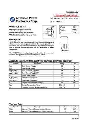
AP6N100JV Halogen-Free Product Advanced Power N-CHANNEL ENHANCEMENT MODE Electronics Corp. POWER MOSFET 100% Rg & UIS Test D BVDSS 60V Simple Drive Requirement RDS(ON) 100m Fast Switching Characteristic ID 7.5A G RoHS Compliant & Halogen-Free S Description AP6N100 series are from Advanced Power innovated design and silicon process technology to achieve the lowest p... See More ⇒
g06n10.pdf
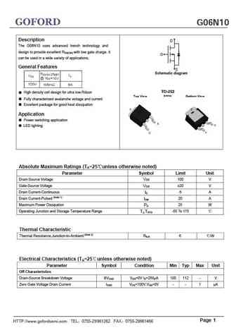
GOFORD G06N10 Description D The G06N10 uses advanced trench technology and design to provide excellent RDS(ON) with low gate charge. It G can be used in a wide variety of applications. General Features S Schematic diagram High density cell design for ultra low Rdson Fully characterized avalanche voltage and current Excellent package for good heat dissipation A... See More ⇒
16n10.pdf
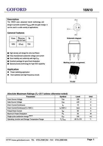
GOFORD 16N10 Description The 16N10 uses advanced trench technology and design to provide excellent RDS(ON) with low gate charge. It can be used in a wide variety of applications. General Features Schematic diagram VDSS RDS(ON) ID @ 10V (typ) 15A 100V 67m High density cell design for ultra low Rdson Fully characterized avalanche voltage and current Good s... See More ⇒
dse026n10n3a.pdf
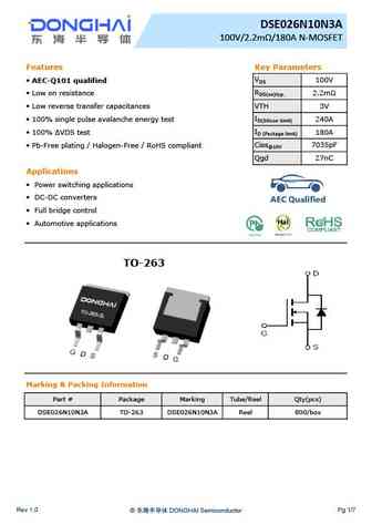
DSE026N10N3A 100V/2.2m /180A N-MOSFET Features Key Parameters VDS AEC-Q101 qualified 100V RDS(on)typ. Low on resistance 2.2m Low reverse transfer capacitances VTH 3V ID(Silicon limit) 100% single pulse avalanche energy test 240A ID (Package limit) 100% VDS test 180A Ciss@10V Pb-Free plating / Halogen-Free / RoHS compliant 7035pF Qgd 27nC Application... See More ⇒
dhs046n10 dhs046n10f dhs046n10i dhs046n10e dhs046n10b dhs046n10d.pdf
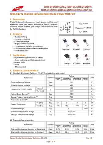
DHS046N10/DHS046N10F/DHS046N10I DHS046N10E/DHS046N10B/DHS046N10D 120A 98V N-channel Enhancement Mode Power MOSFET 1 Description These N-channel enhancement mode power mosfets used 2 D V = 98V DSS advanced splite gate trench technology design, provided excellent Rdson and low gate charge. Which accords with G R = 4.6m DS(on) (TYP) the RoHS standard. 1 3 S I = 120A D 2 Feature... See More ⇒
dse026n10na dsg028n10na.pdf
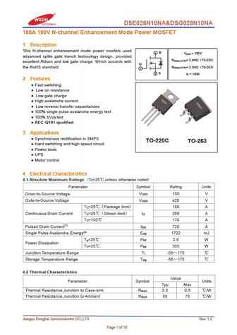
DSE026N10NA&DSG028N10NA 180A 100V N-channel Enhancement Mode Power MOSFET 1 Description This N-channel enhancement mode power mosfets used 2 D V = 100V DSS advanced splite gate trench technology design, provided R = 2.4m T0-220 DS(on) (TYP) excellent Rdson and low gate charge. Which accords with G the RoHS standard. R = 2.2m T0-263 DS(on) (TYP) 1 3 S I = 180A D 2... See More ⇒
utt6n10z.pdf
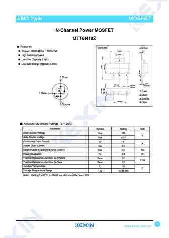
SMD Type MOSFET Transistors N-Channel Power MOSFET UTT6N10Z Features Unit mm SOT-223 6.50 0.2 RDS(on) = 80m @VGS = 10V,ID=6A 3.00 0.1 High Switching Speed Low Crss (Typically 3.1pF) 4 Low Gate Charge (Typically 4.3nC) 1 2 3 2.Drain 0.250 2.30 (typ) 0.84 (max) Gauge Plane 0.66 (min) 1.Gate 1.Gate 2.Drain 3.Source 4.60 (typ) 4.Drain 3.Sou... See More ⇒
blm06n10-p blm06n10-b.pdf
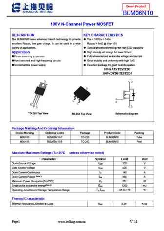
Green Product BLM06N10 100V N-Channel Power MOSFET DESCRIPTION KEY CHARACTERISTICS The BLM06N10 uses advanced trench technology to provide V = 100V,I = 140A DS D excellent R , low gate charge. It can be used in a wide R ... See More ⇒
blm16n10-p blm16n10-d.pdf
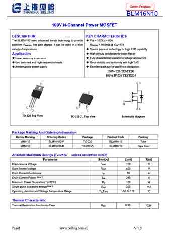
Green Product BLM16N10 100V N-Channel Power MOSFET DESCRIPTION KEY CHARACTERISTICS The BLM16N10 uses advanced trench technology to provide V = 100V,I = 60A DS D excellent R , low gate charge. It can be used in a wide R ... See More ⇒
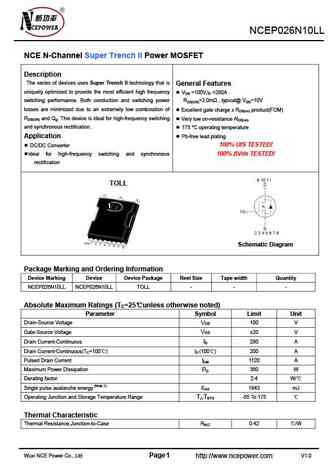
ncep026n10m.pdf
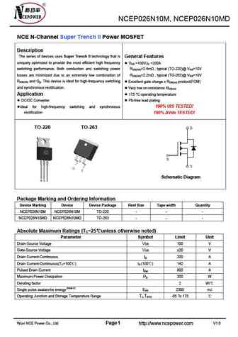
NCEP026N10M, NCEP026N10MD NCE N-Channel Super Trench II Power MOSFET Description The series of devices uses Super Trench II technology that is General Features uniquely optimized to provide the most efficient high frequency VDS =100V,ID =200A switching performance. Both conduction and switching power RDS(ON)=2.4m , typical (TO-220)@ VGS=10V losses are minimized due to an ... See More ⇒
ncep036n10msl.pdf
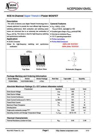
NCEP036N10MSL NCE N-Channel Super Trench II Power MOSFET Description The series of devices uses Super Trench II technology that is General Features uniquely optimized to provide the most efficient high frequency V =100V,I =215A DS D switching performance. Both conduction and switching power R =3.0m , typical@ V =10V DS(ON) GS losses are minimized due to an extremely low combinat... See More ⇒
ncep026n10d.pdf
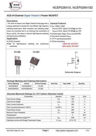
NCEP026N10, NCEP026N10D NCE N-Channel Super Trench II Power MOSFET Description The series of devices uses Super Trench II technology that is General Features uniquely optimized to provide the most efficient high frequency V =100V,I =200A DS D switching performance. Both conduction and switching power R =2.4m , typical (TO-220)@ V =10V DS(ON) GS losses are minimized due to an ext... See More ⇒
ncep016n10ll.pdf
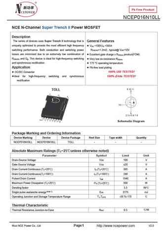
Pb Free Product NCEP016N10LL NCE N-Channel Super Trench II Power MOSFET Description The series of devices uses Super Trench II technology that is General Features uniquely optimized to provide the most efficient high frequency V =100V,I =385A DS D switching performance. Both conduction and switching power R =1.2m , typical@ V =10V DS(ON) GS losses are minimized due to an extrem... See More ⇒
nceap016n10ll.pdf
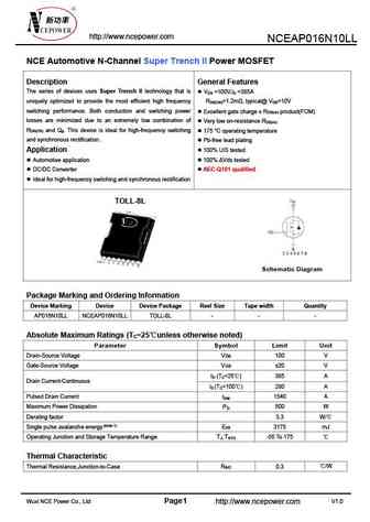
http //www.ncepower.com NCEAP016N10LL NCE Automotive N-Channel Super Trench II Power MOSFET Description General Features The series of devices uses Super Trench II technology that is V =100V,I =385A DS D uniquely optimized to provide the most efficient high frequency R =1.2m , typical@ V =10V DS(ON) GS switching performance. Both conduction and switching power Excellent gate ... See More ⇒
nceap026n10t.pdf
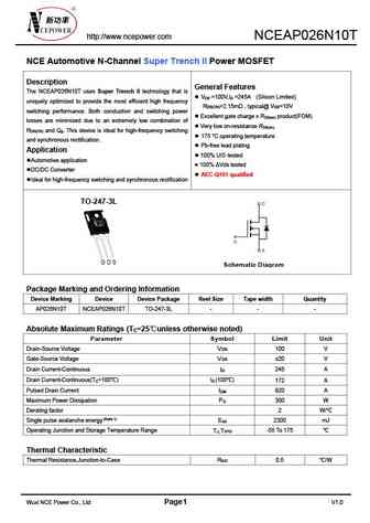
http //www.ncepower.com NCEAP026N10T NCE Automotive N-Channel Super Trench II Power MOSFET Description General Features The NCEAP026N10T uses Super Trench II technology that is V =100V,I =245A (Silicon Limited) DS D uniquely optimized to provide the most efficient high frequency R =2.15m , typical@ V =10V DS(ON) GS switching performance. Both conduction and switching power ... See More ⇒
ncep026n10ll.pdf
NCEP026N10LL NCE N-Channel Super Trench II Power MOSFET Description The series of devices uses Super Trench II technology that is General Features uniquely optimized to provide the most efficient high frequency VDS =100V,ID =280A switching performance. Both conduction and switching power RDS(ON)=2.0m , typical@ VGS=10V losses are minimized due to an extremely low combinat... See More ⇒
ncep026n10t.pdf
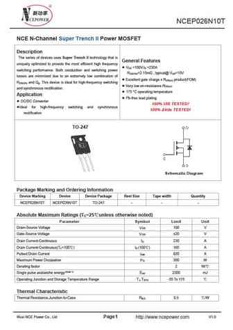
NCEP026N10T NCE N-Channel Super Trench II Power MOSFET Description The series of devices uses Super Trench II technology that is General Features uniquely optimized to provide the most efficient high frequency V =100V,I =230A DS D switching performance. Both conduction and switching power R =2.15m , typical@ V =10V DS(ON) GS losses are minimized due to an extremely low combinat... See More ⇒
ncep026n10 ncep026n10d.pdf

NCEP026N10, NCEP026N10D NCE N-Channel Super Trench II Power MOSFET Description The series of devices uses Super Trench II technology that is General Features uniquely optimized to provide the most efficient high frequency V =100V,I =200A DS D switching performance. Both conduction and switching power R =2.4m , typical (TO-220)@ V =10V DS(ON) GS losses are minimized due to an ext... See More ⇒
ncep026n10f.pdf
NCEP026N10F NCE N-Channel Super Trench II Power MOSFET Description The series of devices uses Super Trench II technology that is General Features uniquely optimized to provide the most efficient high frequency VDS =100V,ID =200A switching performance. Both conduction and switching power RDS(ON)=2.9m , typical @ VGS=10V losses are minimized due to an extremely low combinat... See More ⇒
ncep026n10.pdf

NCEP026N10, NCEP026N10D NCE N-Channel Super Trench II Power MOSFET Description The series of devices uses Super Trench II technology that is General Features uniquely optimized to provide the most efficient high frequency V =100V,I =200A DS D switching performance. Both conduction and switching power R =2.4m , typical (TO-220)@ V =10V DS(ON) GS losses are minimized due to an ext... See More ⇒
hrlfs136n10p.pdf
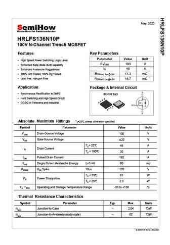
May 2020 HRLFS136N10P 100V N-Channel Trench MOSFET Features Key Parameters Parameter Value Unit High Speed Power Switching, Logic Level BVDSS 100 V Enhanced Body diode dv/dt capability ID 48 A Enhanced Avalanche Ruggedness RDS(on), typ @10V 11.3 m 100% UIS Tested, 100% Rg Tested Lead free, Halogen Free RDS(on), typ @4.5V 16.7 m Application Package & Intern... See More ⇒
wvm6n100.pdf
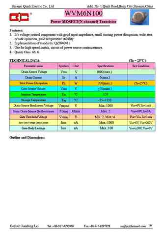
Shaanxi Qunli Electric Co., Ltd Add. No. 1 Qunli Road,Baoji City,Shaanxi,China WVM6N100 Power MOSFET(N-channel) Transistor Features 1. It s voltage control component with good input impedance, small starting power dissipation, wide area of safe operation, good temperature stability. 2. Implementation of standards QZJ840611 3. Use for high speed switch, circuit of power source co... See More ⇒
st36n10d.pdf
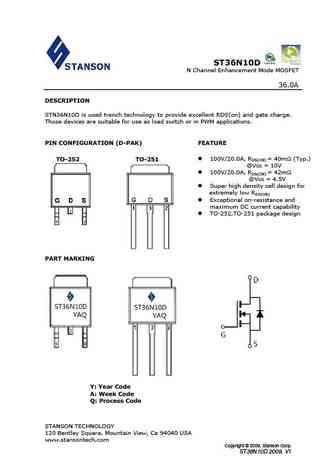
ST36N10D N Channel Enhancement Mode MOSFET 36.0A DESCRIPTION STN36N10D is used trench technology to provide excellent RDS(on) and gate charge. Those devices are suitable for use as load switch or in PWM applications. PIN CONFIGURATION (D-PAK) FEATURE 100V/20.0A, RDS(ON) = 40m (Typ.) TO-252 TO-251 @VGS = 10V 100V/20.0A, RDS(ON) = 42m @VGS = 4.5V Super high densi... See More ⇒
st16n10.pdf
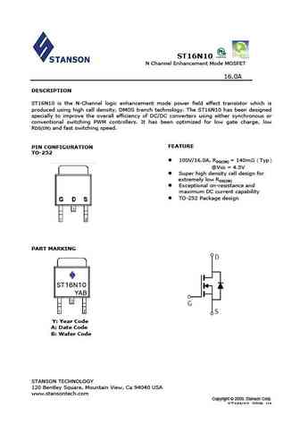
ST16N10 N Channel Enhancement Mode MOSFET 16.0A DESCRIPTION ST16N10 is the N-Channel logic enhancement mode power field effect transistor which is produced using high cell density, DMOS trench technology. The ST16N10 has been designed specially to improve the overall efficiency of DC/DC converters using either synchronous or conventional switching PWM controllers. It has been opt... See More ⇒
wml6n100d1.pdf
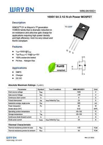
WML6N100D1 1000V 6A 2.1 N-ch Power MOSFET Description TO-220F WMOSTM D1 is Wayon s 1st generation VDMOS family that is dramatic reduction in on-resistance and ultra-low gate charge for applications requiring high power density and high efficiency. And it is very robust and RoHS compliant. Features G V =1050V@T DS jmax D S Typ.R =2.1 @V =10V DS(on)... See More ⇒
wmk16n10t1.pdf
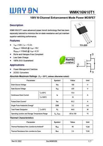
WMK16N10T1 100V N-Channel Enhancement Mode Power MOSFET Description WMK16N10T1 uses advanced power trench technology that has been especially tailored to minimize the on-state resistance and yet maintain superior switching performance. Features S D G V =100V, I = 15.8A DS D TO-220 R ... See More ⇒
wms06n10ts.pdf
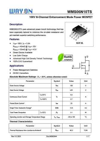
WMS06N10TS 100V N-Channel Enhancement Mode Power MOSFET Description D D D WMS06N10TS uses advanced power trench technology that has D been especially tailored to minimize the on-state resistance and yet maintain superior switching performance. S S S Features G SOP-8L V = 100V, I = 5.8A DS D R ... See More ⇒
cs6n100f cs6n100p cs6n100w.pdf
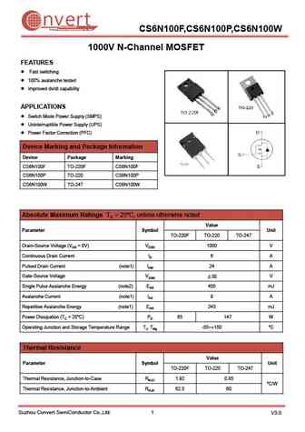
nvert Suzhou Convert Semiconductor Co ., Ltd. CS6N100F,CS6N100P,CS6N100W 1000V N-Channel MOSFET FEATURES Fast switching 100% avalanche tested Improved dv/dt capability APPLICATIONS Switch Mode Power Supply (SMPS) Uninterruptible Power Supply (UPS) Power Factor Correction (PFC) Device Marking and Package Information Device Package Marking CS6N100F TO-220F CS... See More ⇒
hp16n10 hf16n10.pdf
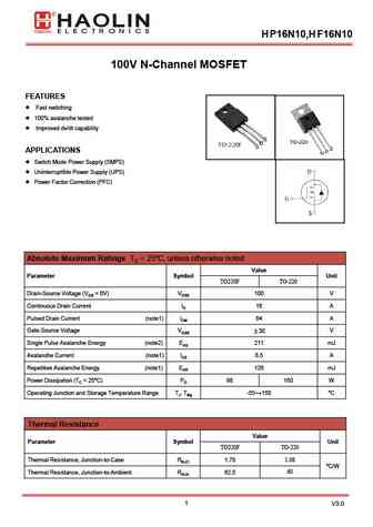
H P16N10,H F16N10 100V N-Channel MOSFET FEATURES Fast switching 100% avalanche tested Improved dv/dt capability APPLICATIONS Switch Mode Power Supply (SMPS) Uninterruptible Power Supply (UPS) Power Factor Correction (PFC) Absolute Maximum Ratings TC = 25 unless otherwise noted C, Value Parameter Symbol Unit TO220F TO-220 Drain-Source Voltage (VGS = 0V) V... See More ⇒
agm056n10c.pdf
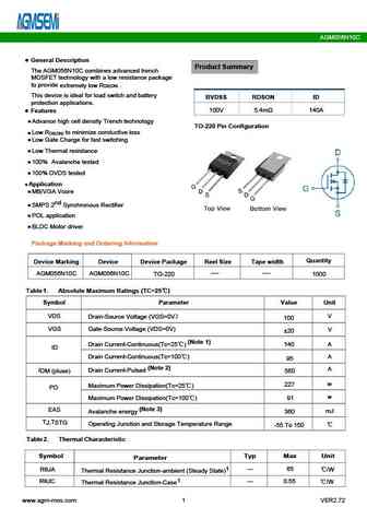
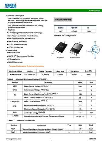
AGM056N10C General Description Product Summary The AGM056N10C combines advanced trench MOSFET technology with a low resistance package to provide extremely low R . DS(ON) This device is ideal switch and battery for load BVDSS RDSON ID protection applications. 100V 5.4m 140A Features Advance high cell density Trench technology TO-220 Pin Configuration Low R to... See More ⇒
agm16n10c.pdf
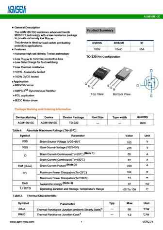
AGM16N10C General Description Product Summary The AGM16N10C combines advanced trench MOSFET technology with a low resistance package to provide extremely low R . DS(ON) This device is ideal for load switch and battery BVDSS RDSON ID protection applications. Features 100V 15m 55A Advance high cell density Trench technology TO-220 Pin Configuration Low R to minimi... See More ⇒
agm056n10h.pdf
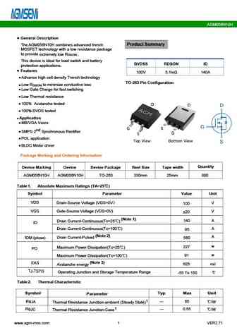
AGM056N10H General Description The AGM056N10H combines advanced trench Product Summary MOSFET technology with a low resistance package to provide extremely low R . DS(ON) This device is ideal switch and battery for load BVDSS RDSON ID protection applications. Features 100V 5.1m 140A Advance high cell density Trench technology TO-263 Pin Configuration Low R to ... See More ⇒
agm16n10d.pdf
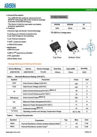
AGM16N10D General Description Product Summary The AGM16N10D combines advanced trench MOSFET technology with a low resistance package to provide extremely low R . DS(ON) This device is ideal for load switch and battery BVDSS RDSON ID protection applications. Features 100V 16m 40A Advance high cell density Trench technology TO-252 Pin Configuration Low R to minimi... See More ⇒
agm056n10a.pdf
AGM056N10A General Description The AGM056N10A combines advanced trench Product Summary MOSFET technology with a low resistance package to provide extremely low R . DS(ON) device is ideal This for load switch and battery protection applications. BVDSS RDSON ID Features 100V 4.7m 100A Advance high cell density Trench technology PDFN5*6 Pin Configuration Low R to ... See More ⇒
wsp06n10.pdf
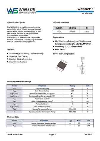
WSP06N10 N-Ch MOSFET General Description Product Summery The WSP06N10 is the highest performance BVDSS RDSON ID trench N-Ch MOSFET with extreme high cell density,which provide excellent RDSON and 100V 85m 4.5A gate charge for most of the synchronous buck converter applications . Applications The WSP06N10 meet the RoHS and Green Product requirement , 100% EAS guaranteed ... See More ⇒
wsp16n10.pdf
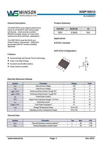
WSP16N10 N-Ch MOSFET General Description Product Summery The WSP16N10 is the highest performance BVDSS RDSON ID trench N-Ch MOSFET with extreme high cell density , which provide excellent 100V 8.9m 16A RDSON and gate charge for most of the synchronous buck converter applications . Applications The WSF16N10 meet the RoHS and Green Product requirement , 100% EAS DC/DC ... See More ⇒
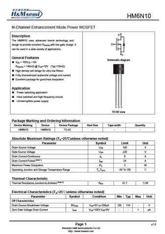
hm6n10r.pdf
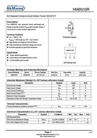
HM6N10R N-Channel Enhancement Mode Power MOSFET Description D The HM6N10R uses advanced trench technology and design to provide excellent RDS(ON) with low gate charge. It G can be used in a wide variety of applications. S General Features VDS = 100V,ID = 6A Schematic diagram RDS(ON) ... See More ⇒
sfp046n100c3 sfb044n100c3.pdf
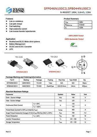
SFP046N100C3,SFB044N100C3 N-MOSFET 100V, 3.6m , 120A Features Product Summary Low on resistance V 100V DS Low gate charge R 3.6m DS(on) typ. Fast switching I 120A D High avalanche current Low reverse transfer capacitances 100% DVDS Tested Application 100% Avalanche Tested Brushed and BLDC Motor drive systems Battery Management DC/DC ... See More ⇒
sfp026n100c3 sfb024n100c3.pdf
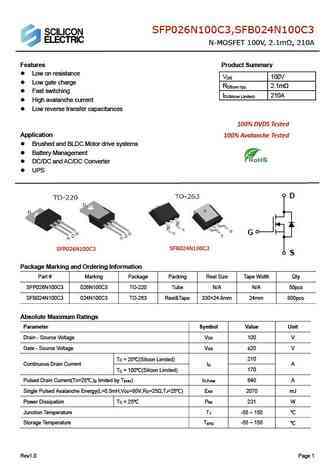
SFP026N100C3,SFB024N100C3 N-MOSFET 100V, 2.1m , 210A Features Product Summary Low on resistance V 100V DS Low gate charge R 2.1m DS(on) typ. Fast switching I 210A D(Silicon Limited) High avalanche current Low reverse transfer capacitances 100% DVDS Tested Application 100% Avalanche Tested Brushed and BLDC Motor drive systems Battery Manage... See More ⇒
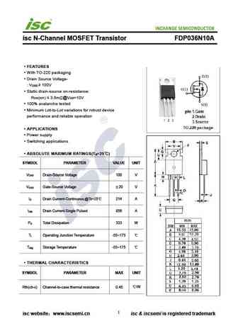
fdp036n10a.pdf

isc N-Channel MOSFET Transistor FDP036N10A FEATURES With TO-220 packaging Drain Source Voltage- V 100V DSS Static drain-source on-resistance RDS(on) 4.5m @V =10V GS 100% avalanche tested Minimum Lot-to-Lot variations for robust device performance and reliable operation APPLICATIONS Power supply Switching applications ABSOLUTE MAXIMUM RATINGS(T =25... See More ⇒
fdp036n10a .pdf
isc N-Channel MOSFET Transistor FDP036N10A FEATURES With TO-220 packaging Drain Source Voltage- V 100V DSS Static drain-source on-resistance RDS(on) 3.6m @V =10V GS 100% avalanche tested Minimum Lot-to-Lot variations for robust device performance and reliable operation APPLICATIONS Power supply Switching applications ABSOLUTE MAXIMUM RATINGS(T =25... See More ⇒
ipa086n10n3.pdf
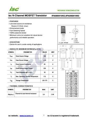
isc N-Channel MOSFET Transistor IPA086N10N3,IIPA086N10N3 FEATURES Low drain-source on-resistance RDS(on) 4.5m (max) Enhancement mode Fast Switching Speed 100% avalanche tested Minimum Lot-to-Lot variations for robust device performance and reliable operation DESCRITION Device for use in a wide variety of applications ABSOLUTE MAXIMUM RATINGS(T =25 ) a SY... See More ⇒
fdi036n10a.pdf
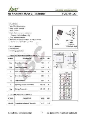
isc N-Channel MOSFET Transistor FDI036N10A FEATURES With TO-262 packaging Drain Source Voltage- V 100V DSS Static drain-source on-resistance RDS(on) 4.5m @V =10V GS 100% avalanche tested Minimum Lot-to-Lot variations for robust device performance and reliable operation APPLICATIONS Power supply Switching applications ABSOLUTE MAXIMUM RATINGS(T =25... See More ⇒
ipp126n10n3.pdf
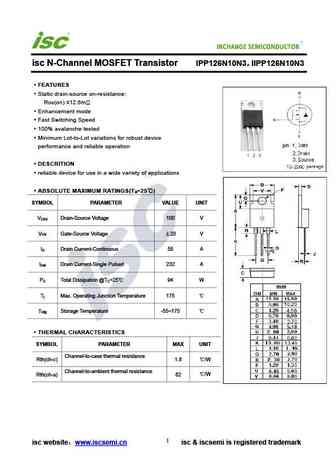
INCHANGE Semiconductor isc N-Channel MOSFET Transistor IPP126N10N3 IIPP126N10N3 FEATURES Static drain-source on-resistance RDS(on) 12.6m Enhancement mode Fast Switching Speed 100% avalanche tested Minimum Lot-to-Lot variations for robust device performance and reliable operation DESCRITION reliable device for use in a wide variety of applications ABSOLUT... See More ⇒
ipi086n10n3.pdf
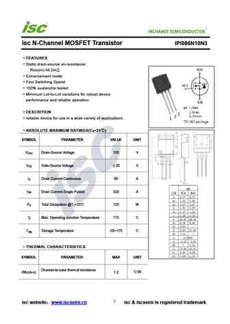
INCHANGE Semiconductor isc N-Channel MOSFET Transistor IPI086N10N3 FEATURES Static drain-source on-resistance RDS(on) 8.2m Enhancement mode Fast Switching Speed 100% avalanche tested Minimum Lot-to-Lot variations for robust device performance and reliable operation DESCRITION reliable device for use in a wide variety of applications ABSOLUTE MAXIMUM RATINGS(... See More ⇒
ipp086n10n3.pdf
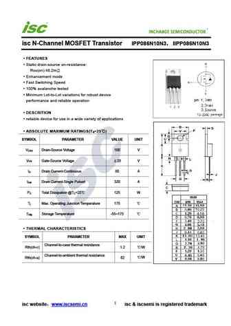
INCHANGE Semiconductor isc N-Channel MOSFET Transistor IPP086N10N3 IIPP086N10N3 FEATURES Static drain-source on-resistance RDS(on) 8.2m Enhancement mode Fast Switching Speed 100% avalanche tested Minimum Lot-to-Lot variations for robust device performance and reliable operation DESCRITION reliable device for use in a wide variety of applications ABSOLUTE ... See More ⇒
ap6n10mi.pdf
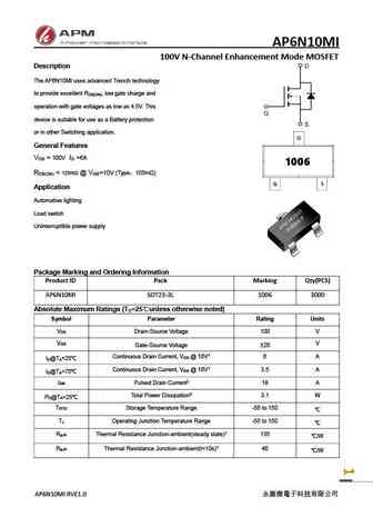
AP6N10MI 100V N-Channel Enhancement Mode MOSFET Description The AP6N10MI uses advanced Trench technology to provide excellent R , low gate charge and DS(ON) operation with gate voltages as low as 4.5V. This device is suitable for use as a Battery protection or in other Switching application. General Features V = 100V I =6A DS D R ... See More ⇒
Detailed specifications: 19N10 , 22N20 , 25N06 , 25N10 , 30N06 , 50N06 , 60N06 , 60N08 , EMB04N03H , 70N06 , 75N75 , 7N10 , 7N10Z , 80N08 , UF1010A , UF1010E , UF3710 .
Keywords - 6N10 MOSFET specs
6N10 cross reference
6N10 equivalent finder
6N10 pdf lookup
6N10 substitution
6N10 replacement
Step-by-step guide to finding a MOSFET replacement. Cross-reference parts and ensure compatibility for your repair or project.


LIST
Last Update
MOSFET: AOT66613L | AOSP21313C | AOSP21311C | AOB66918L | AO3415C | AOTF20N40L | AOTF11N60L | AOT11N60L | AONS21303C | AOI280A60
Popular searches
2n333 | c3852 | irfp140 | ksc2383 datasheet | 2n3906 equivalent | a733 transistor equivalent | 2n5401 transistor datasheet | 2n2222 data sheet