MTN2510J3 Specs and Replacement
Type Designator: MTN2510J3
Type of Transistor: MOSFET
Type of Control Channel: N-Channel
Absolute Maximum Ratings
Pd ⓘ - Maximum Power Dissipation: 130 W
|Vds|ⓘ - Maximum Drain-Source Voltage: 100 V
|Vgs|ⓘ - Maximum Gate-Source Voltage: 20 V
|Id| ⓘ - Maximum Drain Current: 50 A
Tj ⓘ - Maximum Junction Temperature: 175 °C
Electrical Characteristics
tr ⓘ - Rise Time: 100 nS
Cossⓘ - Output Capacitance: 218 pF
RDSonⓘ - Maximum Drain-Source On-State Resistance: 0.019 Ohm
Package: TO-252
MTN2510J3 substitution
- MOSFET ⓘ Cross-Reference Search
MTN2510J3 datasheet
mtn2510j3.pdf
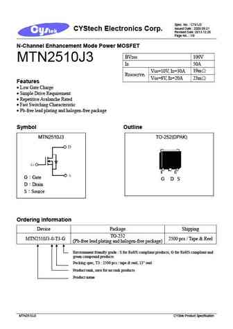
Spec. No. C741J3 Issued Date 2009.09.21 CYStech Electronics Corp. Revised Date 2013.12.26 Page No. 1/9 N-Channel Enhancement Mode Power MOSFET BVDSS 100V MTN2510J3 ID 50A 19m VGS=10V, ID=30A RDSON(TYP) 23m VGS=6V, ID=20A Features Low Gate Charge Simple Drive Requirement Repetitive Avalanche Rated Fast Switching Characteristic Pb... See More ⇒
mtn2510le3.pdf
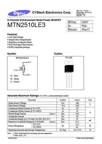
Spec. No. C741E3 Issued Date 2012.03.07 CYStech Electronics Corp. Revised Date Page No. 1/6 N-Channel Enhancement Mode Power MOSFET BVDSS 100V ID 50A MTN2510LE3 RDS(ON) 30m Features Low Gate Charge Simple Drive Requirement Repetitive Avalanche Rated Fast Switching Characteristic RoHS compliant package Symbol Outline TO-220 MTN2510... See More ⇒
mtn2510lj3.pdf
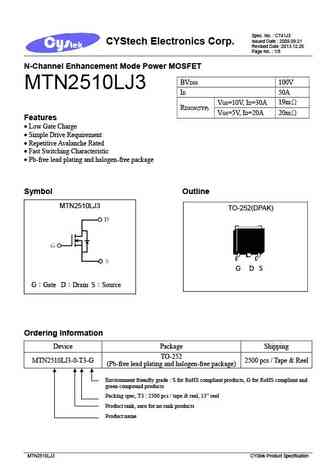
Spec. No. C741J3 Issued Date 2009.09.21 CYStech Electronics Corp. Revised Date 2013.12.26 Page No. 1/8 N-Channel Enhancement Mode Power MOSFET BVDSS 100V MTN2510LJ3 ID 50A 19m VGS=10V, ID=30A RDSON(TYP) 20m VGS=5V, ID=20A Features Low Gate Charge Simple Drive Requirement Repetitive Avalanche Rated Fast Switching Characteristic P... See More ⇒
mtn2510h8.pdf
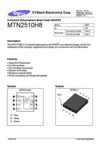
Spec. No. C741H8 Issued Date 2013.07.04 CYStech Electronics Corp. Revised Date 2013.09.14 Page No. 1/11 N-Channel Enhancement Mode Power MOSFET BVDSS 100V MTN2510H8 ID 55A 17m VGS=10V, ID=30A RDSON(TYP) 21m VGS=6V, ID=20A Description The MTN2510H8 is a N-channel enhancement-mode MOSFET, providing the designer with the best combination of fast switching, ... See More ⇒
Detailed specifications: MTN2310N3, MTN2310V8, MTN2328M3, MTN2328N3, MTN2342N3, MTN2510E3, MTN2510F3, MTN2510H8, IRF1407, MTN2510LE3, MTN2510LJ3, MTN2572F3, MTN2572FP, MTN2572H8, MTN2572J3, MTN2604G6, MTN2N60FP
Keywords - MTN2510J3 MOSFET specs
MTN2510J3 cross reference
MTN2510J3 equivalent finder
MTN2510J3 pdf lookup
MTN2510J3 substitution
MTN2510J3 replacement
Need a MOSFET replacement? Our guide shows you how to find a perfect substitute by comparing key parameters and specs
