AOB262L Datasheet. Specs and Replacement
Type Designator: AOB262L 📄📄
Type of Transistor: MOSFET
Type of Control Channel: N-Channel
Absolute Maximum Ratings
Pd ⓘ - Maximum Power Dissipation: 333 W
|Vds|ⓘ - Maximum Drain-Source Voltage: 60 V
|Vgs|ⓘ - Maximum Gate-Source Voltage: 20 V
|Id| ⓘ - Maximum Drain Current: 140 A
Tj ⓘ - Maximum Junction Temperature: 175 °C
Electrical Characteristics
tr ⓘ - Rise Time: 22 nS
Cossⓘ - Output Capacitance: 1040 pF
RDSonⓘ - Maximum Drain-Source On-State Resistance: 0.0028 Ohm
Package: TO-263
📄📄 Copy
- MOSFET ⓘ Cross-Reference Search
AOB262L datasheet
..1. Size:333K aosemi
aob262l.pdf 
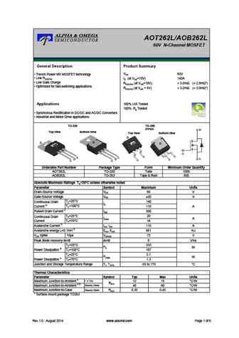
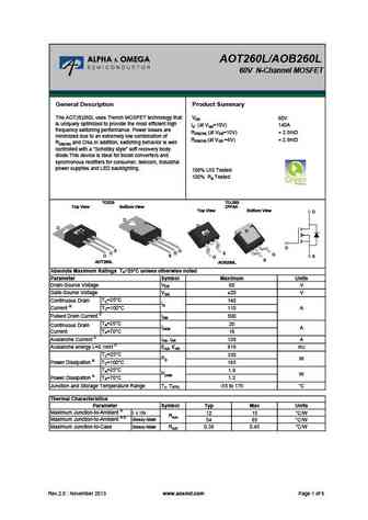
AOT262L/AOB262L 60V N-Channel MOSFET General Description Product Summary VDS 60V Trench Power MV MOSFET technology Low RDS(ON) ID (at VGS=10V) 140A Low Gate Charge RDS(ON) (at VGS=10V) ... See More ⇒
..2. Size:238K inchange semiconductor
aob262l.pdf
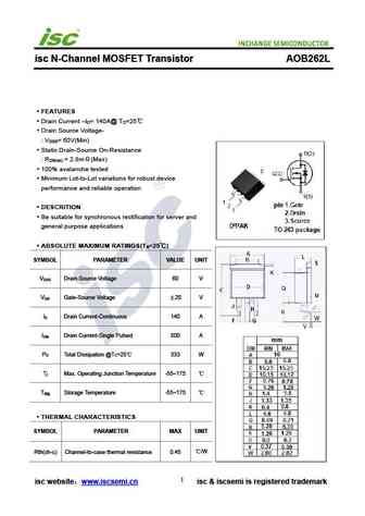
isc N-Channel MOSFET Transistor AOB262L FEATURES Drain Current I = 140A@ T =25 D C Drain Source Voltage- V = 60V(Min) DSS Static Drain-Source On-Resistance R = 2.8m (Max) DS(on) 100% avalanche tested Minimum Lot-to-Lot variations for robust device performance and reliable operation DESCRITION Be suitable for synchronous rectification for server and gene... See More ⇒
9.1. Size:424K aosemi
aot2618l aob2618l aotf2618l.pdf
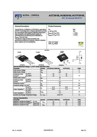
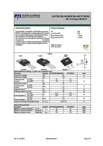
AOT2618L/AOB2618L/AOTF2618L 60V N-Channel MOSFET General Description Product Summary VDS The AOT2618L & AOB2618L & AOTF2618L uses trench 60V MOSFET technology that is uniquely optimized to provide ID (at VGS=10V) 23A the most efficient high frequency switching performance. RDS(ON) (at VGS=10V) ... See More ⇒
9.2. Size:276K aosemi
aob260l.pdf
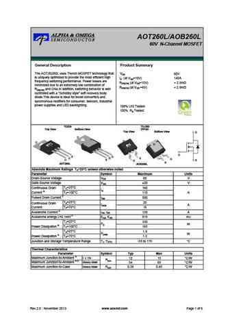
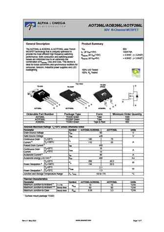
AOT260L/AOB260L 60V N-Channel MOSFET General Description Product Summary The AOT(B)260L uses Trench MOSFET technology that VDS 60V is uniquely optimized to provide the most efficient high ID (at VGS=10V) 140A frequency switching performance. Power losses are RDS(ON) (at VGS=10V) ... See More ⇒
9.3. Size:367K aosemi
aob2618l.pdf
AOT2618L/AOB2618L/AOTF2618L 60V N-Channel MOSFET General Description Product Summary VDS The AOT2618L & AOB2618L & AOTF2618L uses trench 60V MOSFET technology that is uniquely optimized to provide ID (at VGS=10V) 23A the most efficient high frequency switching performance. RDS(ON) (at VGS=10V) ... See More ⇒
9.4. Size:420K aosemi
aot2606l aob2606l aotf2606l.pdf
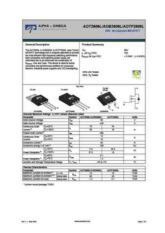
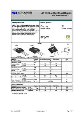
AOT2606L/AOB2606L/AOTF2606L 60V N-Channel MOSFET General Description Product Summary VDS The AOT2606L & AOB2606L & AOTF2606L uses Trench 60V MOSFET technology that is uniquely optimized to provide ID (at VGS=10V) 72A the most efficient high frequency switching performance. RDS(ON) (at VGS=10V) ... See More ⇒
9.5. Size:358K aosemi
aob264l aot264l.pdf

AOT264L/AOB264L 60V N-Channel MOSFET General Description Product Summary VDS 60V The AOT264L/AOB264L combines advanced trench MOSFET technology with a low resistance package to ID (at VGS=10V) 140A provide extremely low RDS(ON).This device is ideal for boost RDS(ON) (at VGS=10V) ... See More ⇒
9.6. Size:289K aosemi
aob2608l.pdf
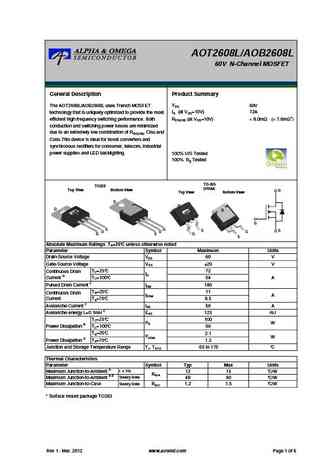
AOT2608L/AOB2608L 60V N-Channel MOSFET General Description Product Summary VDS The AOT2608L/AOB2608L uses Trench MOSFET 60V ID (at VGS=10V) 72A technology that is uniquely optimized to provide the most efficient high frequency switching performance. Both RDS(ON) (at VGS=10V) ... See More ⇒
9.7. Size:349K aosemi
aob2606l.pdf
AOT2606L/AOB2606L/AOTF2606L 60V N-Channel MOSFET General Description Product Summary VDS The AOT2606L & AOB2606L & AOTF2606L uses Trench 60V MOSFET technology that is uniquely optimized to provide ID (at VGS=10V) 72A the most efficient high frequency switching performance. RDS(ON) (at VGS=10V) ... See More ⇒
9.8. Size:405K aosemi
aob266l.pdf
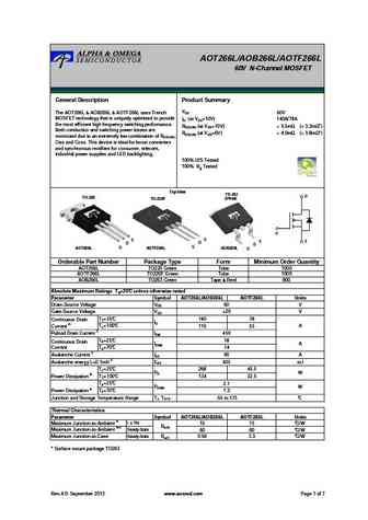
AOT266L/AOB266L/AOTF266L 60V N-Channel MOSFET General Description Product Summary VDS The AOT266L & AOB266L & AOTF266L uses Trench 60V MOSFET technology that is uniquely optimized to provide ID (at VGS=10V) 140A/78A the most efficient high frequency switching performance. RDS(ON) (at VGS=10V) ... See More ⇒
9.9. Size:414K aosemi
aot266l aob266l aotf266l.pdf
AOT266L/AOB266L/AOTF266L 60V N-Channel MOSFET General Description Product Summary VDS The AOT266L & AOB266L & AOTF266L uses Trench 60V MOSFET technology that is uniquely optimized to ID (at VGS=10V) 140A/78A provide the most efficient high frequency switching RDS(ON) (at VGS=10V) ... See More ⇒
9.10. Size:358K aosemi
aot264l aob264l.pdf
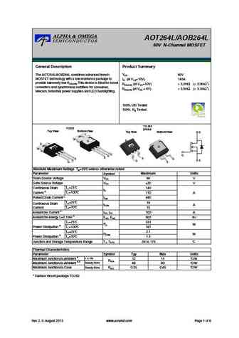
AOT264L/AOB264L 60V N-Channel MOSFET General Description Product Summary VDS 60V The AOT264L/AOB264L combines advanced trench MOSFET technology with a low resistance package to ID (at VGS=10V) 140A provide extremely low RDS(ON).This device is ideal for boost RDS(ON) (at VGS=10V) ... See More ⇒
9.11. Size:402K aosemi
aot260l aob260l.pdf
AOT260L/AOB260L 60V N-Channel MOSFET General Description Product Summary The AOT(B)260L uses Trench MOSFET technology that VDS 60V is uniquely optimized to provide the most efficient high ID (at VGS=10V) 140A frequency switching performance. Power losses are RDS(ON) (at VGS=10V) ... See More ⇒
9.12. Size:257K inchange semiconductor
aob260l.pdf
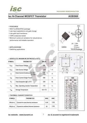
Isc N-Channel MOSFET Transistor AOB260l FEATURES With To-263(D2PAK) package Low input capacitance and gate charge Low gate input resistance 100% avalanche tested Minimum Lot-to-Lot variations for robust device performance and reliable operation APPLICATIONS Switching applications ABSOLUTE MAXIMUM RATINGS(T =25 ) a SYMBOL PARAMETER VALUE UNIT V Drain-Source Volta... See More ⇒
9.13. Size:238K inchange semiconductor
aob2618l.pdf
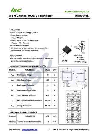
isc N-Channel MOSFET Transistor AOB2618L FEATURES Drain Current I = 23A@ T =25 D C Drain Source Voltage- V = 60V(Min) DSS Static Drain-Source On-Resistance R = 19m (Max) DS(on) 100% avalanche tested Minimum Lot-to-Lot variations for robust device performance and reliable operation DESCRITION Be suitable for synchronous rectification for server and gener... See More ⇒
9.14. Size:238K inchange semiconductor
aob2608l.pdf
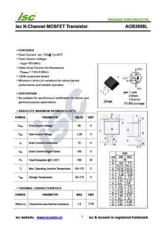
isc N-Channel MOSFET Transistor AOB2608L FEATURES Drain Current I = 72A@ T =25 D C Drain Source Voltage- V = 60V(Min) DSS Static Drain-Source On-Resistance R = 7.6m (Max) DS(on) 100% avalanche tested Minimum Lot-to-Lot variations for robust device performance and reliable operation DESCRITION Be suitable for synchronous rectification for server and gene... See More ⇒
9.15. Size:264K inchange semiconductor
aob2606l.pdf
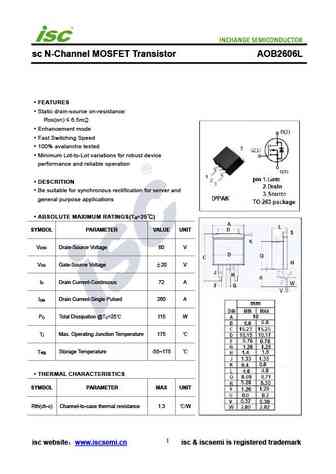
sc N-Channel MOSFET Transistor AOB2606L FEATURES Static drain-source on-resistance RDS(on) 6.5m Enhancement mode Fast Switching Speed 100% avalanche tested Minimum Lot-to-Lot variations for robust device performance and reliable operation DESCRITION Be suitable for synchronous rectification for server and general purpose applications ABSOLUTE MAXIMUM RATING... See More ⇒
9.16. Size:203K inchange semiconductor
aob266l.pdf
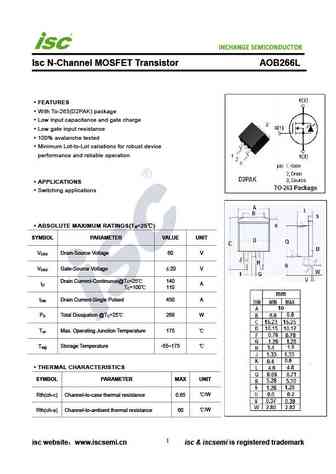
INCHANGE Semiconductor Isc N-Channel MOSFET Transistor AOB266L FEATURES With To-263(D2PAK) package Low input capacitance and gate charge Low gate input resistance 100% avalanche tested Minimum Lot-to-Lot variations for robust device performance and reliable operation APPLICATIONS Switching applications ABSOLUTE MAXIMUM RATINGS(T =25 ) a SYMBOL PARAMETER VALUE UN... See More ⇒
9.17. Size:238K inchange semiconductor
aob264l.pdf

isc N-Channel MOSFET Transistor AOB264L FEATURES Drain Current I = 140A@ T =25 D C Drain Source Voltage- V = 60V(Min) DSS Static Drain-Source On-Resistance R = 3m (Max) DS(on) 100% avalanche tested Minimum Lot-to-Lot variations for robust device performance and reliable operation DESCRITION Be suitable for synchronous rectification for server and genera... See More ⇒
Detailed specifications: AOB2500L, AOB254L, AOB256L, AOB25S65, AOB2606L, AOB2608L, AOB260L, AOB2618L, 8205A, AOB264L, AOB266L, AOB270AL, AOB27S60, AOB280L, AOB282L, AOB284L, AOB286L
Keywords - AOB262L MOSFET specs
AOB262L cross reference
AOB262L equivalent finder
AOB262L pdf lookup
AOB262L substitution
AOB262L replacement
Can't find your MOSFET?
Learn how to find a substitute transistor by analyzing voltage, current and package compatibility
