AOD409 Specs and Replacement
Type Designator: AOD409
Type of Transistor: MOSFET
Type of Control Channel: P-Channel
Absolute Maximum Ratings
Pd ⓘ
- Maximum Power Dissipation: 60 W
|Vds|ⓘ - Maximum Drain-Source Voltage: 60 V
|Vgs|ⓘ - Maximum Gate-Source Voltage: 20 V
|Id| ⓘ - Maximum Drain Current: 26 A
Tj ⓘ - Maximum Junction Temperature: 175 °C
Electrical Characteristics
tr ⓘ - Rise Time: 14.5 nS
Cossⓘ -
Output Capacitance: 241 pF
RDSonⓘ - Maximum Drain-Source On-State Resistance: 0.04 Ohm
Package: TO-252
- MOSFET ⓘ Cross-Reference Search
AOD409 datasheet
..1. Size:383K aosemi
aod409.pdf 
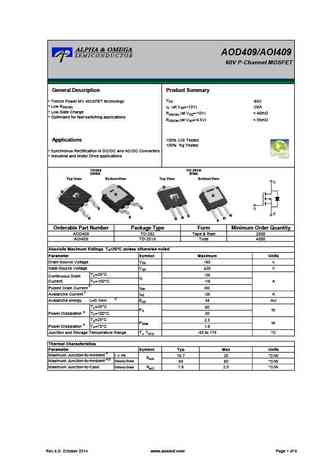
AOD409/AOI409 60V P-Channel MOSFET General Description Product Summary VDS Trench Power MV MOSFET technology -60V Low RDS(ON) ID (at VGS=-10V) -26A Low Gate Charge RDS(ON) (at VGS=-10V) ... See More ⇒
..2. Size:237K aosemi
aod409 aoi409.pdf
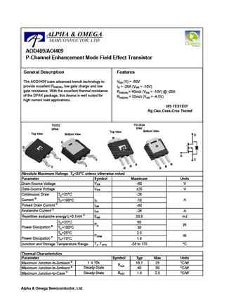
AOD409/AOI409 P-Channel Enhancement Mode Field Effect Transistor General Description Features The AOD/I409 uses advanced trench technology to VDS (V) = -60V provide excellent RDS(ON), low gate charge and low ID = -26A (VGS = -10V) gate resistance. With the excellent thermal resistance RDS(ON) ... See More ⇒
..3. Size:207K inchange semiconductor
aod409.pdf
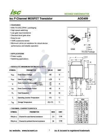
INCHANGE Semiconductor isc P-Channel MOSFET Transistor AOD409 FEATURES With TO-252( DPAK ) packaging High speed switching Low gate input resistance Standard level gate drive Easy to use 100% avalanche tested Minimum Lot-to-Lot variations for robust device performance and reliable operation APPLICATIONS Power supply Switching applications ABSOLUTE MAXIMUM RA... See More ⇒
0.1. Size:317K aosemi
aod409g.pdf
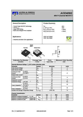
AOD409G 60V P-Channel MOSFET General Description Product Summary VDS Trench Power MOSFET technology -60V Low RDS(ON) ID (at VGS=-10V) -28A Logic Level Driving RDS(ON) (at VGS=-10V) ... See More ⇒
0.2. Size:249K inchange semiconductor
aod409g.pdf
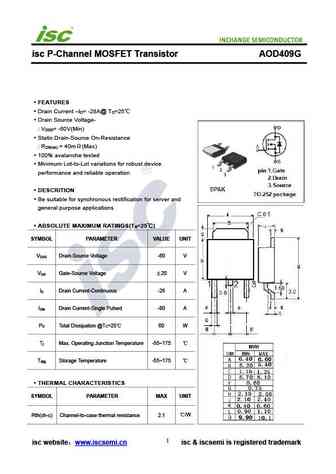
isc P-Channel MOSFET Transistor AOD409G FEATURES Drain Current I = -28A@ T =25 D C Drain Source Voltage- V = -60V(Min) DSS Static Drain-Source On-Resistance R = 40m (Max) DS(on) 100% avalanche tested Minimum Lot-to-Lot variations for robust device performance and reliable operation DESCRITION Be suitable for synchronous rectification for server and gene... See More ⇒
9.1. Size:111K aosemi
aod408.pdf
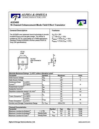
AOD408 N-Channel Enhancement Mode Field Effect Transistor General Description Features The AOD408 uses advanced trench technology to provide VDS (V) = 30V excellent RDS(ON) and low gate charge. This device is ID = 18A (VGS = 10V) suitable for use as a load switch or in PWM applications. RDS(ON) ... See More ⇒
9.2. Size:195K aosemi
aod404.pdf
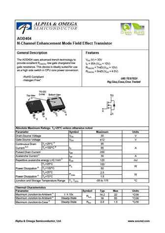
AOD404 N-Channel Enhancement Mode Field Effect Transistor General Description Features The AOD404 uses advanced trench technology to VDS (V) = 30V provide excellent RDS(ON), low gate chargeand low ID = 85A (VGS = 10V) gate resistance. This device is ideally suited for use RDS(ON) ... See More ⇒
9.3. Size:398K aosemi
aod403 aoi403.pdf

AOD403/AOI403 30V P-Channel MOSFET General Description Product Summary VDS -30V The AOD403/AOI403 uses advanced trench technology to provide excellent RDS(ON), low gate charge and low gate ID (at VGS= -20V) -70A resistance. With the excellent thermal resistance of the RDS(ON) (at VGS= -20V) ... See More ⇒
9.4. Size:244K aosemi
aod402.pdf
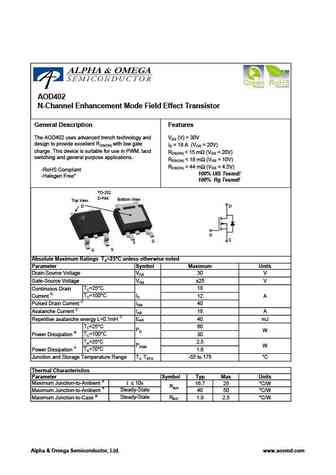
AOD402 N-Channel Enhancement Mode Field Effect Transistor General Description Features The AOD402 uses advanced trench technology and VDS (V) = 30V design to provide excellent RDS(ON) with low gate ID = 18 A (VGS = 20V) charge. This device is suitable for use in PWM, laod RDS(ON) ... See More ⇒
9.5. Size:210K aosemi
aod400.pdf
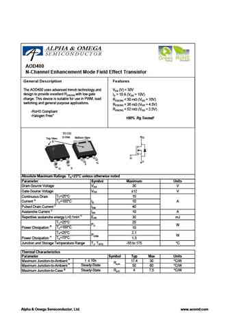
AOD400 N-Channel Enhancement Mode Field Effect Transistor General Description Features The AOD400 uses advanced trench technology and VDS (V) = 30V design to provide excellent RDS(ON) with low gate ID = 10 A (VGS = 10V) charge. This device is suitable for use in PWM, load RDS(ON) ... See More ⇒
9.6. Size:196K aosemi
aod406.pdf
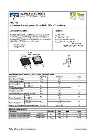
AOD406 N-Channel Enhancement Mode Field Effect Transistor General Description Features The AOD406 uses advanced trench technology to provide VDS (V) = 30V excellent RDS(ON), shoot-through immunity and body diode ID = 85A (VGS = 10V) characteristics. This device is ideally suited for use as a low RDS(ON) ... See More ⇒
9.7. Size:398K aosemi
aod403.pdf
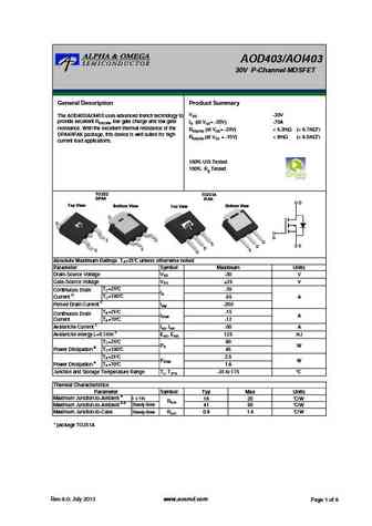
AOD403/AOI403 30V P-Channel MOSFET General Description Product Summary VDS -30V The AOD403/AOI403 uses advanced trench technology to provide excellent RDS(ON), low gate charge and low gate ID (at VGS= -20V) -70A resistance. With the excellent thermal resistance of the RDS(ON) (at VGS= -20V) ... See More ⇒
9.8. Size:154K aosemi
aod407.pdf
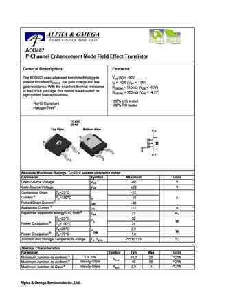
AOD407 P-Channel Enhancement Mode Field Effect Transistor General Description Features The AOD407 uses advanced trench technology to VDS (V) = -60V provide excellent RDS(ON), low gate charge and low ID = -12A (VGS = -10V) gate resistance. With the excellent thermal resistance RDS(ON) ... See More ⇒
9.9. Size:841K cn vbsemi
aod408.pdf

AOD408 www.VBsemi.tw N-Channel 30-V (D-S) MOSFET FEATURES PRODUCT SUMMARY TrenchFET Power MOSFET VDS (V) RDS(on) ( ) ID (A)a, e Qg (Typ) 100 % Rg and UIS Tested Compliant to RoHS Directive 2011/65/EU 0.007 at VGS = 10 V 50 30 25 nC 0.009 at VGS = 4.5 V 40 APPLICATIONS D OR-ing Server TO-252 DC/DC G G D S S Top View N-Channel MOSFET ABSOLUT... See More ⇒
9.10. Size:841K cn vbsemi
aod400.pdf
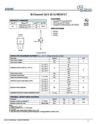
AOD400 www.VBsemi.tw N-Channel 30-V (D-S) MOSFET FEATURES PRODUCT SUMMARY TrenchFET Power MOSFET VDS (V) RDS(on) ( ) ID (A)a, e Qg (Typ) 100 % Rg and UIS Tested Compliant to RoHS Directive 2011/65/EU 0.007 at VGS = 10 V 50 30 25 nC 0.009 at VGS = 4.5 V 40 APPLICATIONS D OR-ing Server TO-252 DC/DC G G D S S Top View N-Channel MOSFET ABSOLUT... See More ⇒
9.11. Size:838K cn vbsemi
aod406.pdf
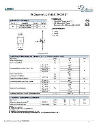
AOD406 www.VBsemi.tw N-Channel 30-V (D-S) MOSFET FEATURES PRODUCT SUMMARY TrenchFET Power MOSFET VDS (V) RDS(on) ( ) ID (A)a, e Qg (Typ) 100 % Rg and UIS Tested Compliant to RoHS Directive 2011/65/EU 0.002 at VGS = 10 V 100 30 72 nC 0.003 at VGS = 4.5 V 90 APPLICATIONS D OR-ing Server TO-252 DC/DC G G D S Top View S N-Channel MOSFET ABSOLU... See More ⇒
9.12. Size:840K cn vbsemi
aod403.pdf
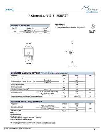
AOD403 www.VBsemi.tw P-Channel 30 V (D-S) MOSFET FEATURES PRODUCT SUMMARY Compliant to RoHS Directive 2002/95/EC VDS (V) RDS(on) ( )ID (A)a Available 0.009 at VGS = - 10 V 80 RoHS* - 30 COMPLIANT 0.012 at VGS = - 4.5 V 80 S TO-252 G D G S D Top View P-Channel MOSFET ABSOLUTE MAXIMUM RATINGS (TC = 25 C, unless otherwise noted) Parameter Symbol Limit Unit Gat... See More ⇒
9.13. Size:830K cn vbsemi
aod407.pdf
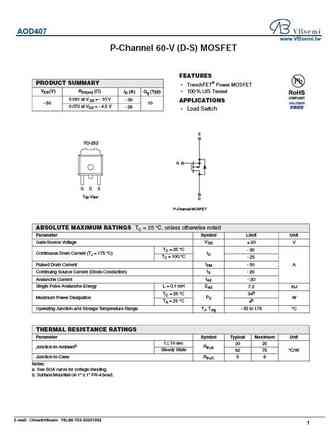
AOD407 www.VBsemi.tw P-Channel 60-V (D-S) MOSFET FEATURES PRODUCT SUMMARY TrenchFET Power MOSFET VDS (V) RDS(on) ( ) ID (A) Qg (Typ) 100 % UIS Tested 0.061 at VGS = - 10 V - 30 APPLICATIONS - 60 10 0.072 at VGS = - 4.5 V - 26 Load Switch S TO-252 G G D S Top View D P-Channel MOSFET ABSOLUTE MAXIMUM RATINGS TC = 25 C, unless otherwise noted Parameter Symbol... See More ⇒
9.14. Size:241K inchange semiconductor
aod403.pdf
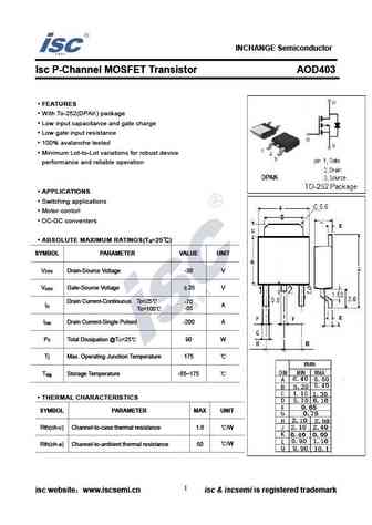
INCHANGE Semiconductor Isc P-Channel MOSFET Transistor AOD403 FEATURES With To-252(DPAK) package Low input capacitance and gate charge Low gate input resistance 100% avalanche tested Minimum Lot-to-Lot variations for robust device performance and reliable operation APPLICATIONS Switching applications Motor contorl DC-DC conventers ABSOLUTE MAXIMUM RATINGS(T =2... See More ⇒
9.15. Size:265K inchange semiconductor
aod407.pdf
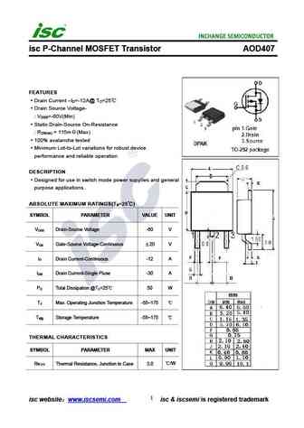
isc P-Channel MOSFET Transistor AOD407 FEATURES Drain Current I =-12A@ T =25 D C Drain Source Voltage- V =-60V(Min) DSS Static Drain-Source On-Resistance R = 115m (Max) DS(on) 100% avalanche tested Minimum Lot-to-Lot variations for robust device performance and reliable operation DESCRIPTION Designed for use in switch mode power supplies and general purpose... See More ⇒
Detailed specifications: AOD2N60A, AOD3N40, AOD3N50, AOD3N60, AOD3N80, AOD3T40P, AOD403, AOD407, IRF730, AOD4102, AOD4120, AOD4124, AOD4126, AOD4128, AOD4130, AOD4132, AOD4136
Keywords - AOD409 MOSFET specs
AOD409 cross reference
AOD409 equivalent finder
AOD409 pdf lookup
AOD409 substitution
AOD409 replacement
Step-by-step guide to finding a MOSFET replacement. Cross-reference parts and ensure compatibility for your repair or project.
