APT6025BLL Datasheet. Specs and Replacement
Type Designator: APT6025BLL
Type of Transistor: MOSFET
Type of Control Channel: N-Channel
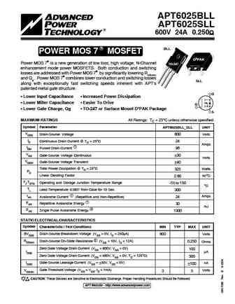
Absolute Maximum Ratings
Pd ⓘ - Maximum Power Dissipation: 325 W
|Vds|ⓘ - Maximum Drain-Source Voltage: 600 V
|Vgs|ⓘ - Maximum Gate-Source Voltage: 30 V
|Id| ⓘ - Maximum Drain Current: 24 A
Tj ⓘ - Maximum Junction Temperature: 150 °C
Electrical Characteristics
tr ⓘ - Rise Time: 8 nS
Cossⓘ - Output Capacitance: 480 pF
RDSonⓘ - Maximum Drain-Source On-State Resistance: 0.25 Ohm
Package: TO247
APT6025BLL substitution
- MOSFET ⓘ Cross-Reference Search
APT6025BLL datasheet
apt6025bll.pdf
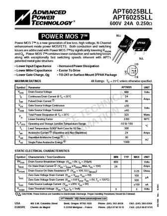
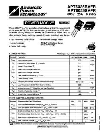
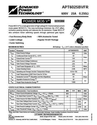
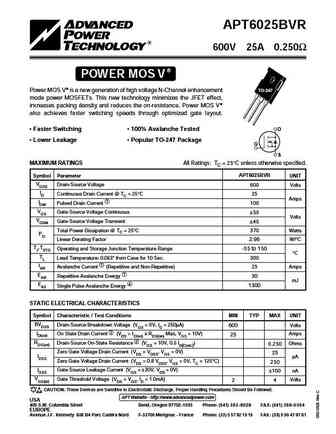
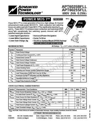
APT6025BLL APT6025SLL 600V 24A 0.250W TM BLL POWER MOS 7 Power MOS 7TM is a new generation of low loss, high voltage, N-Channel D3PAK TO-247 enhancement mode power MOSFETS. Both conduction and switching losses are addressed with Power MOS 7TM by significantly lowering RDS(ON) and Qg. Power MOS 7TM combines lower conduction and switching losses along with exceptionally fast switching ... See More ⇒
apt6025bll.pdf
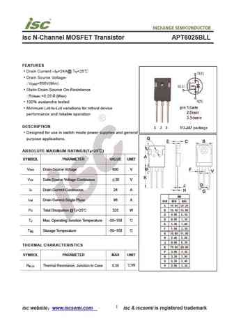
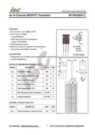
isc N-Channel MOSFET Transistor APT6025BLL FEATURES Drain Current I =24A@ T =25 D C Drain Source Voltage- V =600V(Min) DSS Static Drain-Source On-Resistance R =0.25 (Max) DS(on) 100% avalanche tested Minimum Lot-to-Lot variations for robust device performance and reliable operation DESCRIPTION Designed for use in switch mode power supplies and general purpo... See More ⇒
apt6025bllg.pdf
APT6025BLL APT6025SLL 600V 24A 0.250 R BLL POWER MOS 7 MOSFET D3PAK Power MOS 7 is a new generation of low loss, high voltage, N-Channel TO-247 enhancement mode power MOSFETS. Both conduction and switching losses are addressed with Power MOS 7 by significantly lowering RDS(ON) and Qg. Power MOS 7 combines lower conduction and switching losses SLL along... See More ⇒
apt6025bfllg apt6025sfllg.pdf
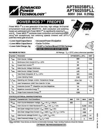
APT6025BFLL APT6025SFLL 600V 24A 0.250 BFLL R POWER MOS 7 FREDFET D3PAK Power MOS 7 is a new generation of low loss, high voltage, N-Channel TO-247 enhancement mode power MOSFETS. Both conduction and switching losses are addressed with Power MOS 7 by significantly lowering RDS(ON) and Qg. Power MOS 7 combines lower conduction and switching losses SFLL ... See More ⇒


Detailed specifications: APT6015LVFR, APT6017B2FLL, APT6017B2LL, APT6017JFLL, APT6017JLL, APT6021BFLL, APT6021BLL, APT6025BFLL, 8205A, APT6025BVFR, APT6025SVFR, APT6025SVR, APT6029BFLL, APT6029BLL, APT6030BVFR, APT6030SVFR, APT6030SVR
Keywords - APT6025BLL MOSFET specs
APT6025BLL cross reference
APT6025BLL equivalent finder
APT6025BLL pdf lookup
APT6025BLL substitution
APT6025BLL replacement
Learn how to find the right MOSFET substitute. A guide to cross-reference, check specs and replace MOSFETs in your circuits.
History: IXFR80N10Q
🌐 : EN ES РУ

LIST
Last Update
MOSFET: ASDM40N60KQ | ASDM40N40E | ASDM40N100P | ASDM40DN20E | ASDM3416EZA | ASDM3415ZA | ASDM3401ZA | ASDM3401 | ASDM3400ZA | ASDM30P30BE
Popular searches
bu406 datasheet | irfb7437 | tip32a | p75nf75 mosfet equivalent | irfpe50 | tip50 | transistor bc547 datasheet | bc109c