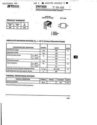
2N7005 Specs and Replacement
Type Designator: 2N7005
Type of Transistor: MOSFET
Type of Control Channel: N-Channel
Absolute Maximum Ratings
Pd ⓘ - Maximum Power Dissipation: 1 W
|Vds|ⓘ - Maximum Drain-Source Voltage: 200 V
|Vgs|ⓘ - Maximum Gate-Source Voltage: 20 V
|Id| ⓘ - Maximum Drain Current: 0.6 A
Tj ⓘ - Maximum Junction Temperature: 150 °C
Electrical Characteristics
tr ⓘ - Rise Time: 18 nS
Cossⓘ - Output Capacitance: 65 pF
RDSonⓘ - Maximum Drain-Source On-State Resistance: 1.5 Ohm
Package: TO250
2N7005 substitution
- MOSFET ⓘ Cross-Reference Search
2N7005 datasheet
2n7002lt1.pdf
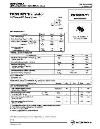
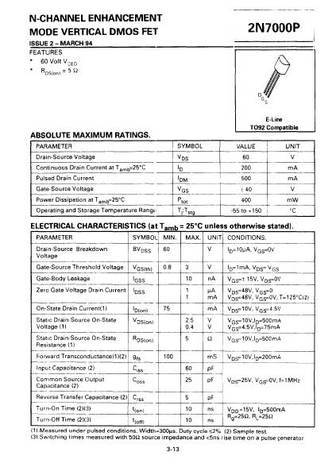
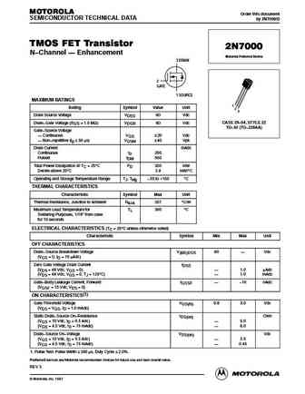
MOTOROLA Order this document SEMICONDUCTOR TECHNICAL DATA by 2N7002LT1/D TMOS FET Transistor 2N7002LT1 3 DRAIN N Channel Enhancement Motorola Preferred Device 1 GATE 3 2 SOURCE 1 MAXIMUM RATINGS 2 Rating Symbol Value Unit Drain Source Voltage VDSS 60 Vdc CASE 318 08, STYLE 21 SOT 23 (TO 236AB) Drain Gate Voltage (RGS = 1.0 M ) VDGR 60 Vdc Drain Current Con... See More ⇒
2n7002lt1rev2.pdf

MOTOROLA Order this document SEMICONDUCTOR TECHNICAL DATA by 2N7002LT1/D TMOS FET Transistor 2N7002LT1 3 DRAIN N Channel Enhancement Motorola Preferred Device 1 GATE 3 2 SOURCE 1 MAXIMUM RATINGS 2 Rating Symbol Value Unit Drain Source Voltage VDSS 60 Vdc CASE 318 08, STYLE 21 SOT 23 (TO 236AB) Drain Gate Voltage (RGS = 1.0 M ) VDGR 60 Vdc Drain Current Con... See More ⇒
2n7000r3.pdf
MOTOROLA Order this document SEMICONDUCTOR TECHNICAL DATA by 2N7000/D TMOS FET Transistor 2N7000 N Channel Enhancement Motorola Preferred Device 3 DRAIN 2 GATE 1 SOURCE MAXIMUM RATINGS 1 Rating Symbol Value Unit 2 3 Drain Source Voltage VDSS 60 Vdc CASE 29 04, STYLE 22 Drain Gate Voltage (RGS = 1.0 M ) VDGR 60 Vdc TO 92 (TO 226AA) Gate Source Voltage ... See More ⇒
2n7002.pdf
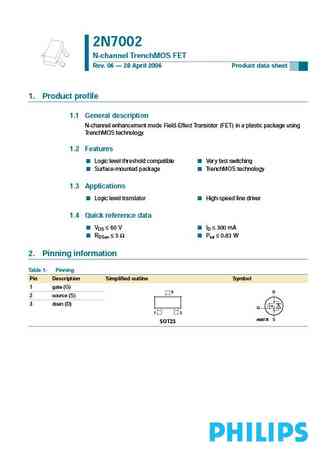
2N7002 N-channel TrenchMOS FET Rev. 06 28 April 2006 Product data sheet 1. Product profile 1.1 General description N-channel enhancement mode Field-Effect Transistor (FET) in a plastic package using TrenchMOS technology. 1.2 Features Logic level threshold compatible Very fast switching Surface-mounted package TrenchMOS technology 1.3 Applications Logic level translator High-sp... See More ⇒
2n7002e.pdf

2N7002E N-channel TrenchMOS FET Rev. 03 28 April 2006 Product data sheet 1. Product profile 1.1 General description N-channel enhancement mode Field-Effect Transistor (FET) in a plastic package using TrenchMOS technology. 1.2 Features Logic level threshold compatible Very fast switching Surface-mounted package TrenchMOS technology 1.3 Applications Logic level translator High-s... See More ⇒
2n7002-03.pdf
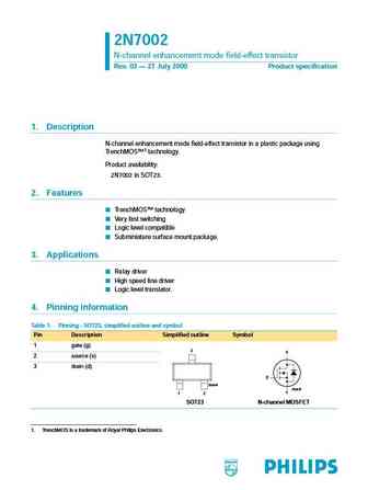
2N7002 N-channel enhancement mode field-effect transistor Rev. 03 27 July 2000 Product specification 1. Description N-channel enhancement mode field-effect transistor in a plastic package using TrenchMOS 1 technology. Product availability 2N7002 in SOT23. 2. Features TrenchMOS technology Very fast switching Logic level compatible Subminiature surface mount package. 3.... See More ⇒
2n7002ps.pdf
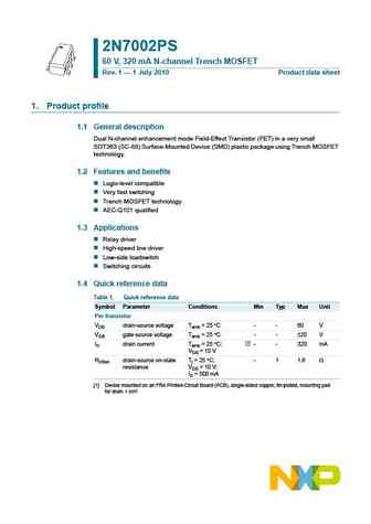
2N7002PS 60 V, 320 mA N-channel Trench MOSFET Rev. 1 1 July 2010 Product data sheet 1. Product profile 1.1 General description Dual N-channel enhancement mode Field-Effect Transistor (FET) in a very small SOT363 (SC-88) Surface-Mounted Device (SMD) plastic package using Trench MOSFET technology. 1.2 Features and benefits Logic-level compatible Very fast switching Trench MOSF... See More ⇒
2n7002p.pdf
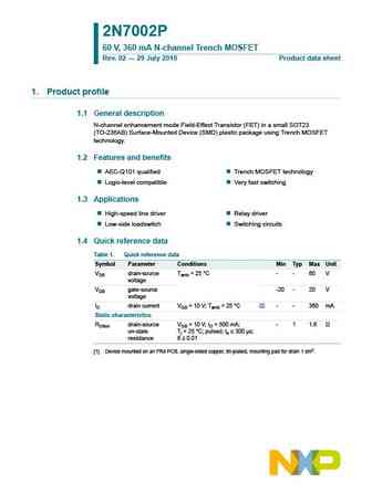
2N7002P 60 V, 360 mA N-channel Trench MOSFET Rev. 02 29 July 2010 Product data sheet 1. Product profile 1.1 General description N-channel enhancement mode Field-Effect Transistor (FET) in a small SOT23 (TO-236AB) Surface-Mounted Device (SMD) plastic package using Trench MOSFET technology. 1.2 Features and benefits AEC-Q101 qualified Trench MOSFET technology Logic-level compat... See More ⇒
2n7002bkt.pdf
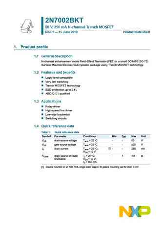
2N7002BKT 60 V, 290 mA N-channel Trench MOSFET Rev. 1 15 June 2010 Product data sheet 1. Product profile 1.1 General description N-channel enhancement mode Field-Effect Transistor (FET) in a small SOT416 (SC-75) Surface-Mounted Device (SMD) plastic package using Trench MOSFET technology. 1.2 Features and benefits Logic-level compatible Very fast switching Trench MOSFET technol... See More ⇒
2n7002ck.pdf
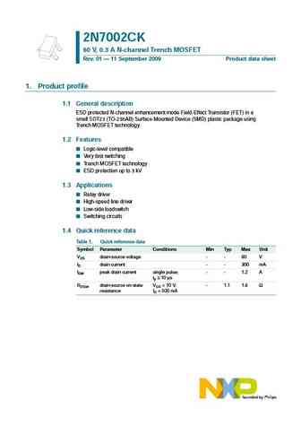
2N7002CK 60 V, 0.3 A N-channel Trench MOSFET Rev. 01 11 September 2009 Product data sheet 1. Product profile 1.1 General description ESD protected N-channel enhancement mode Field-Effect Transistor (FET) in a small SOT23 (TO-236AB) Surface-Mounted Device (SMD) plastic package using Trench MOSFET technology. 1.2 Features Logic-level compatible Very fast switching Trench MOSFET ... See More ⇒
2n7002pt.pdf
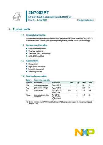
2N7002PT 60 V, 310 mA N-channel Trench MOSFET Rev. 1 2 July 2010 Product data sheet 1. Product profile 1.1 General description N-channel enhancement mode Field-Effect Transistor (FET) in a small SOT416 (SC-75) Surface-Mounted Device (SMD) plastic package using Trench MOSFET technology. 1.2 Features and benefits Logic-level compatible Very fast switching Trench MOSFET ... See More ⇒
2n7002ka.pdf
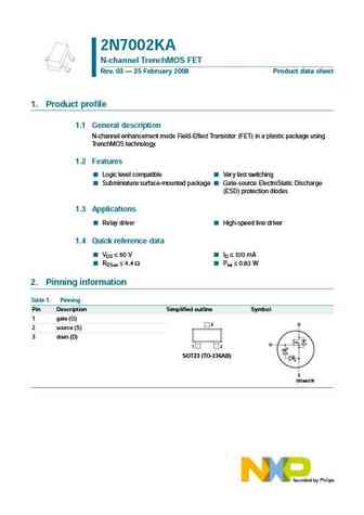
2N7002KA N-channel TrenchMOS FET Rev. 03 25 February 2008 Product data sheet 1. Product profile 1.1 General description N-channel enhancement mode Field-Effect Transistor (FET) in a plastic package using TrenchMOS technology. 1.2 Features Logic level compatible Very fast switching Subminiature surface-mounted package Gate-source ElectroStatic Discharge (ESD) protection diodes 1... See More ⇒
2n7000-03.pdf
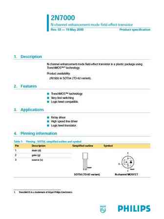
2N7000 N-channel enhancement mode field-effect transistor Rev. 03 19 May 2000 Product specification 1. Description N-channel enhancement mode field-effect transistor in a plastic package using TrenchMOS 1 technology. Product availability 2N7000 in SOT54 (TO-92 variant). 2. Features TrenchMOS technology Very fast switching Logic level compatible. 3. Applications Relay ... See More ⇒
2n7002pw.pdf
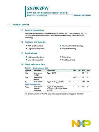
2N7002PW 60 V, 310 mA N-channel Trench MOSFET Rev. 02 29 July 2010 Product data sheet 1. Product profile 1.1 General description N-channel enhancement mode Field-Effect Transistor (FET) in a very small SOT323 (SC-70) Surface-Mounted Device (SMD) plastic package using Trench MOSFET technology. 1.2 Features and benefits AEC-Q101 qualified Trench MOSFET technology Logic-level co... See More ⇒
2n7000 2n7002.pdf
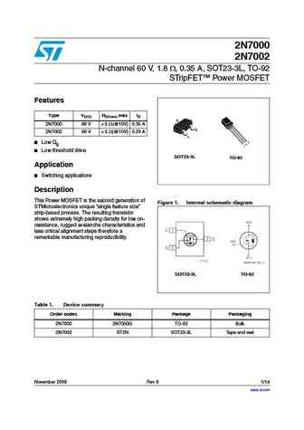
2N7000 2N7002 N-channel 60 V, 1.8 , 0.35 A, SOT23-3L, TO-92 STripFET Power MOSFET Features Type VDSS RDS(on) max ID 3 2N7000 60 V ... See More ⇒
t2n7002bk.pdf
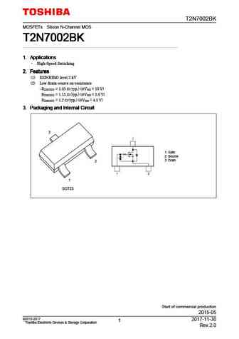
T2N7002BK MOSFETs Silicon N-Channel MOS T2N7002BK T2N7002BK T2N7002BK T2N7002BK 1. Applications 1. Applications 1. Applications 1. Applications High-Speed Switching 2. Features 2. Features 2. Features 2. Features (1) ESD(HBM) level 2 kV (2) Low drain-source on-resistance RDS(ON) = 1.05 (typ.) (@VGS = 10 V) RDS(ON) = 1.15 (typ.) (@VGS = 5.0 V) RDS(ON) = 1.2 ... See More ⇒
t2n7002ak.pdf
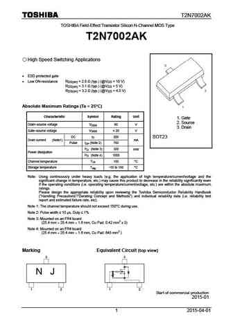
T2N7002AK TOSHIBA Field-Effect Transistor Silicon N-Channel MOS Type T2N7002AK High Speed Switching Applications ESD protected gate Low ON-resistance RDS(on) = 2.8 (typ.) (@VGS = 10 V) RDS(on) = 3.1 (typ.) (@VGS = 5 V) RDS(on) = 3.2 (typ.) (@VGS = 4.5 V) Absolute Maximum Ratings (Ta = 25 C) Characteristic Symbol Rating Unit 1. Gate 2. Source Drai... See More ⇒
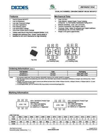
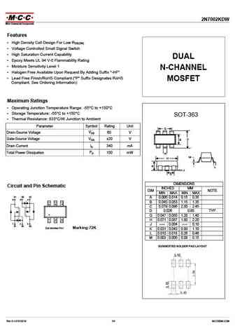
2n7002dw.pdf
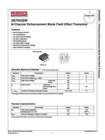
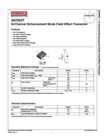
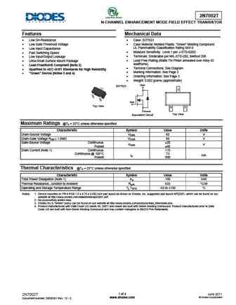
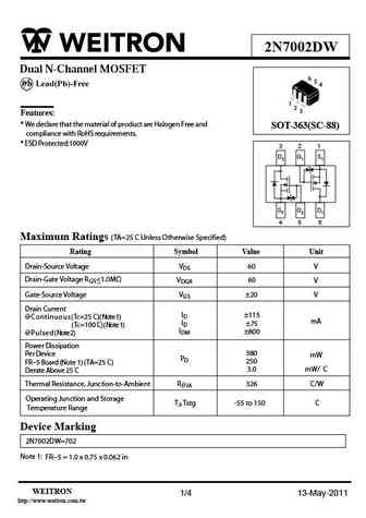
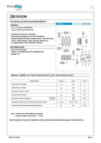
October 2007 2N7002DW N-Channel Enhancement Mode Field Effect Transistor Features Dual N-Channel MOSFET Low On-Resistance Low Gate Threshold Voltage Low Input Capacitance Fast Switching Speed Low Input/Output Leakage Ultra-Small Surface Mount Package Lead Free/RoHS Compliant SC70-6 (SOT363) 1 1 Marking 2N Absolute Maximum Ratings * Ta = 25 C un... See More ⇒
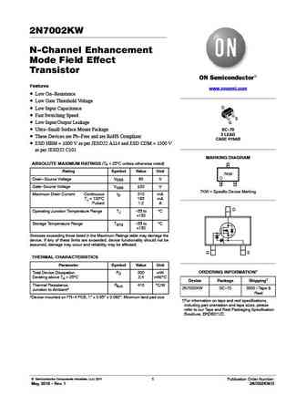
2n7002kw.pdf
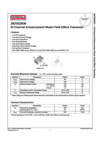
May 2011 2N7002KW N-Channel Enhancement Mode Field Effect Transistor Features Low On-Resistance Low Gate Threshold Voltage Low Input Capacitance Fast Switching Speed Low Input/Output Leakage Ultra-Small Surface Mount Package Pb Free/RoHS Compliant ESD HBM=1000V as per JESD22 A114 and ESD CDM=1500V as per JESD22 C101 D S SOT-323 G Marking 7KW Ab... See More ⇒
2n7000 2n7002 nds7002a.pdf
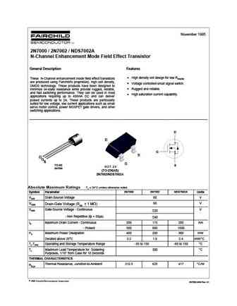
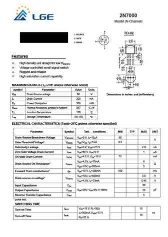
November 1995 2N7000 / 2N7002 / NDS7002A N-Channel Enhancement Mode Field Effect Transistor General Description Features High density cell design for low RDS(ON). These N-Channel enhancement mode field effect transistors are produced using Fairchild's proprietary, high cell density, Voltage controlled small signal switch. DMOS technology. These products have been designed to Rugged ... See More ⇒
2n7000.pdf

November 1995 2N7000 / 2N7002 / NDS7002A N-Channel Enhancement Mode Field Effect Transistor General Description Features High density cell design for low RDS(ON). These N-Channel enhancement mode field effect transistors are produced using Fairchild's proprietary, high cell density, Voltage controlled small signal switch. DMOS technology. These products have been designed to Rugged ... See More ⇒
2n7002v-va.pdf
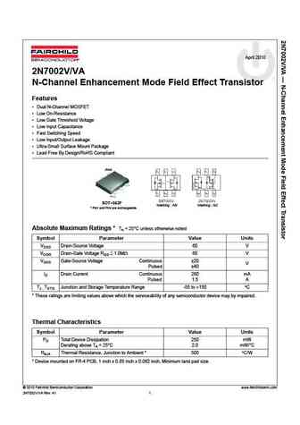
April 2010 2N7002V/VA N-Channel Enhancement Mode Field Effect Transistor Features Dual N-Channel MOSFET Low On-Resistance Low Gate Threshold Voltage Low Input Capacitance Fast Switching Speed Low Input/Output Leakage Ultra-Small Surface Mount Package Lead Free By Design/RoHS Compliant (Pin4) SOT-563F Marking AB Marking AC * Pin1 and Pin4 are ex... See More ⇒
2n7002w.pdf
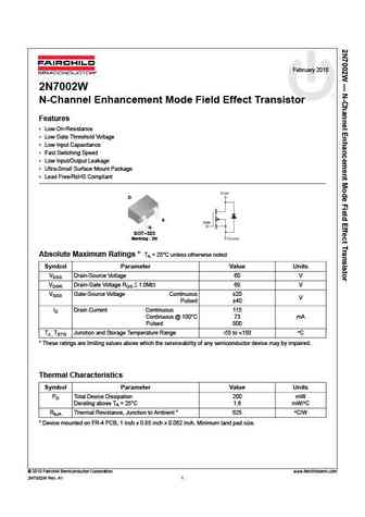
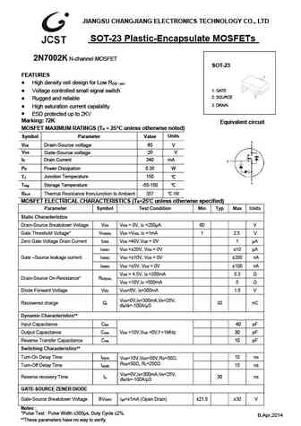
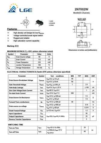
February 2010 2N7002W N-Channel Enhancement Mode Field Effect Transistor Features Low On-Resistance Low Gate Threshold Voltage Low Input Capacitance Fast Switching Speed Low Input/Output Leakage Ultra-Small Surface Mount Package Lead Free/RoHS Compliant D S G SOT-323 Marking 2N Absolute Maximum Ratings * TA = 25 C unless otherwise noted Symbol Par... See More ⇒
2n7002k.pdf
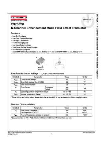
January 2012 2N7002K N-Channel Enhancement Mode Field Effect Transistor Features Low On-Resistance Low Gate Threshold Voltage Low Input Capacitance Fast Switching Speed Low Input/Output Leakage Ultra-Small Surface Mount Package Pb Free/RoHS Compliant ESD HBM=2000V (Typical 3000V) as per JESD22 A114 and ESD CDM=2000V as per JESD22 C101 D S G SOT-23 ... See More ⇒
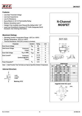
2n7002t.pdf
October 2007 2N7002T N-Channel Enhancement Mode Field Effect Transistor Features Low On-Resistance Low Gate Threshold Voltage Low Input Capacitance Fast Switching Speed Low Input/Output Leakage Ultra-Small Surface Mount Package Lead Free/RoHS Compliant D S G SOT - 523F Marking AA Absolute Maximum Ratings * Ta = 25 C unless otherwise noted Symbol P... See More ⇒
2n7002mtf.pdf
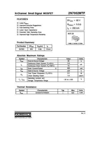
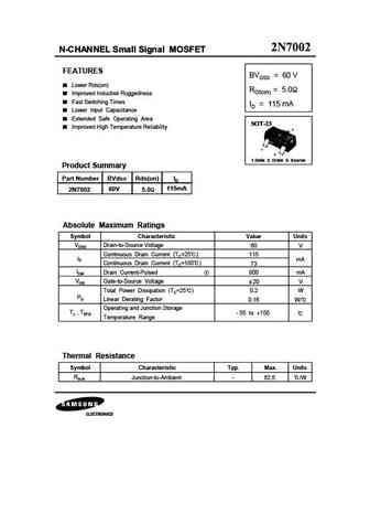
N-Channel Small Signal MOSFET 2N7002MTF FEATURES BVDSS = 60 V Lower RDS(on) RDS(on) = 5.0 Improved Inductive Ruggedness Fast Switching Times ID = 200 mA Lower Input Capacitance Extended Safe Operating Area SOT-23 Improved High Temperature Reliability Product Summary 1.Gate 2. Source 3. Drain Part Number BVDSS RDS(on) ID 2N7002 60V 5.0 115mA Absolute Maximum Ratings ... See More ⇒
2n7000bu.pdf

Advanced Small Signal MOSFET 2N7000BU/2N7000TA FEATURES BVDSS = 60 V n Fast Switching Times RDS(on) = 5.0 n Improved Inductive Ruggedness n Lower Input Capacitance ID = 200 mA n Extended Safe Operating Area n Improved High Temperature Reliability TO-92 1.Source 2. Gate 3. Drain Absolute Maximum Ratings Symbol Characteristic Value Units VDSS Drain-to-Source Voltage V 60 Contin... See More ⇒
2n7000ta.pdf
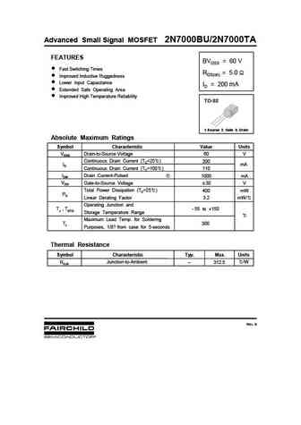
Advanced Small Signal MOSFET 2N7000BU/2N7000TA FEATURES BVDSS = 60 V n Fast Switching Times RDS(on) = 5.0 n Improved Inductive Ruggedness n Lower Input Capacitance ID = 200 mA n Extended Safe Operating Area n Improved High Temperature Reliability TO-92 1.Source 2. Gate 3. Drain Absolute Maximum Ratings Symbol Characteristic Value Units VDSS Drain-to-Source Voltage V 60 Contin... See More ⇒
2n7002bks.pdf

Important notice Dear Customer, On 7 February 2017 the former NXP Standard Product business became a new company with the tradename Nexperia. Nexperia is an industry leading supplier of Discrete, Logic and PowerMOS semiconductors with its focus on the automotive, industrial, computing, consumer and wearable application markets In data sheets and application notes which still contain... See More ⇒
2n7002.pdf
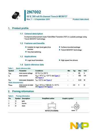
2N7002 60 V, 300 mA N-channel Trench MOSFET Rev. 7 8 September 2011 Product data sheet 1. Product profile 1.1 General description N-channel enhancement mode Field-Effect Transistor (FET) in a plastic package using Trench MOSFET technology. 1.2 Features and benefits Suitable for logic level gate drive Surface-mounted package sources Trench MOSFET technology Very f... See More ⇒
2n7002ps.pdf

Important notice Dear Customer, On 7 February 2017 the former NXP Standard Product business became a new company with the tradename Nexperia. Nexperia is an industry leading supplier of Discrete, Logic and PowerMOS semiconductors with its focus on the automotive, industrial, computing, consumer and wearable application markets In data sheets and application notes which still contain... See More ⇒
2n7002bkv.pdf
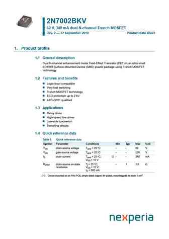
2N7002BKV 60 V, 340 mA dual N-channel Trench MOSFET Rev. 2 22 September 2010 Product data sheet 1. Product profile 1.1 General description Dual N-channel enhancement mode Field-Effect Transistor (FET) in an ultra small SOT666 Surface-Mounted Device (SMD) plastic package using Trench MOSFET technology. 1.2 Features and benefits Logic-level compatible Very fast switching Trenc... See More ⇒
2n7002p.pdf

Important notice Dear Customer, On 7 February 2017 the former NXP Standard Product business became a new company with the tradename Nexperia. Nexperia is an industry leading supplier of Discrete, Logic and PowerMOS semiconductors with its focus on the automotive, industrial, computing, consumer and wearable application markets In data sheets and application notes which still contain... See More ⇒
2n7002ck.pdf
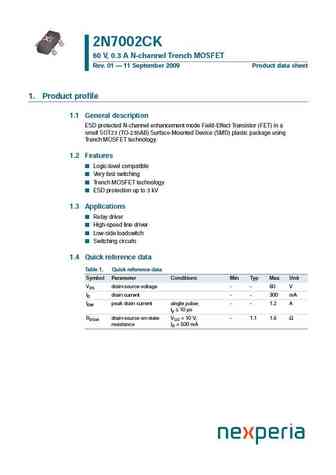
2N7002CK 60 V, 0.3 A N-channel Trench MOSFET Rev. 01 11 September 2009 Product data sheet 1. Product profile 1.1 General description ESD protected N-channel enhancement mode Field-Effect Transistor (FET) in a small SOT23 (TO-236AB) Surface-Mounted Device (SMD) plastic package using Trench MOSFET technology. 1.2 Features Logic-level compatible Very fast switching Trench MOSFET ... See More ⇒
2n7002bkmb.pdf
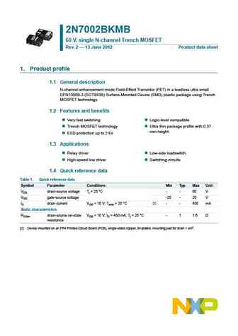
2N7002BKMB 60 V, single N-channel Trench MOSFET Rev. 2 13 June 2012 Product data sheet 1. Product profile 1.1 General description N-channel enhancement mode Field-Effect Transistor (FET) in a leadless ultra small DFN1006B-3 (SOT883B) Surface-Mounted Device (SMD) plastic package using Trench MOSFET technology. 1.2 Features and benefits Very fast switching Logic-level compa... See More ⇒
2n7002bkw.pdf
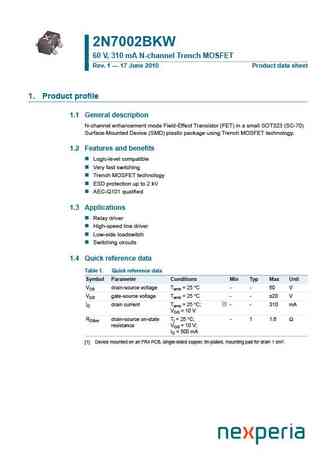
2N7002BKW 60 V, 310 mA N-channel Trench MOSFET Rev. 1 17 June 2010 Product data sheet 1. Product profile 1.1 General description N-channel enhancement mode Field-Effect Transistor (FET) in a small SOT323 (SC-70) Surface-Mounted Device (SMD) plastic package using Trench MOSFET technology. 1.2 Features and benefits Logic-level compatible Very fast switching Trench MOSFET technol... See More ⇒
2n7002pv.pdf
Important notice Dear Customer, On 7 February 2017 the former NXP Standard Product business became a new company with the tradename Nexperia. Nexperia is an industry leading supplier of Discrete, Logic and PowerMOS semiconductors with its focus on the automotive, industrial, computing, consumer and wearable application markets In data sheets and application notes which still contain... See More ⇒
2n7002nxak.pdf
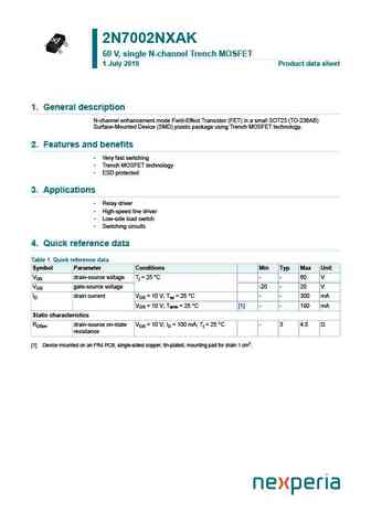
2N7002NXAK 60 V, single N-channel Trench MOSFET 1 July 2019 Product data sheet 1. General description N-channel enhancement mode Field-Effect Transistor (FET) in a small SOT23 (TO-236AB) Surface-Mounted Device (SMD) plastic package using Trench MOSFET technology. 2. Features and benefits Very fast switching Trench MOSFET technology ESD protected 3. Applications Relay ... See More ⇒
2n7002nxbk.pdf
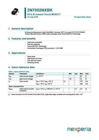
2N7002NXBK 60 V, N-channel Trench MOSFET 25 July 2019 Product data sheet 1. General description N-channel enhancement mode Field-Effect Transistor (FET) in a small SOT23 (TO-236AB) Surface-Mounted Device (SMD) plastic package using Trench MOSFET technology. 2. Features and benefits Logic-level compatible Very fast switching Trench MOSFET technology ElectroStatic Discha... See More ⇒
2n7002pw.pdf

Important notice Dear Customer, On 7 February 2017 the former NXP Standard Product business became a new company with the tradename Nexperia. Nexperia is an industry leading supplier of Discrete, Logic and PowerMOS semiconductors with its focus on the automotive, industrial, computing, consumer and wearable application markets In data sheets and application notes which still contain... See More ⇒
2n7002bk.pdf
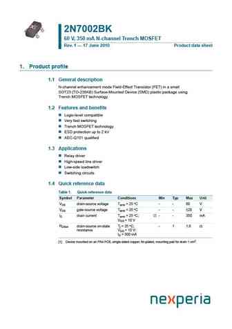
2N7002BK 60 V, 350 mA N-channel Trench MOSFET Rev. 1 17 June 2010 Product data sheet 1. Product profile 1.1 General description N-channel enhancement mode Field-Effect Transistor (FET) in a small SOT23 (TO-236AB) Surface-Mounted Device (SMD) plastic package using Trench MOSFET technology. 1.2 Features and benefits Logic-level compatible Very fast switching Trench MOSFET tech... See More ⇒
2n7002.pdf
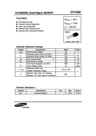
N-CHANNEL SmaII SignaI MOSFET FEATURES BVDSS = 60 V Lower Rds(on) RDS(on) = 5.0 Improved Inductive Ruggedness Fast Switching Times ID = 115 mA Lower Input Capacitance Extended Safe Operating Area SOT-23 Improved High Temperature Reliability 2 1 3 1.Gate 2. Drain 3. Source Product Summary Part Number BVdss Rds(on) ID 115mA 60V 2N7002 5.0 Absolute Maximum Ratings Sy... See More ⇒
2n7000.pdf
N-CHANNEL SmaII SignaI MOSFET FEATURES BVDSS = 60 V Fast Switching Times RDS(on) = 5.0 Improved Inductive Ruggedness Lower Input Capacitance ID = 200 mA Extended Safe Operating Area Improved High Temperature Reliability TO-92 1 2 3 1.Source 2. Gate 3. Drain Absolute Maximum Ratings Symbol Characteristic Value Units VDSS Drain-to-Source Voltage V 60 Continuous Drain Cur... See More ⇒
2n7002e.pdf
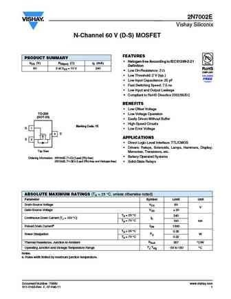
2N7002E Vishay Siliconix N-Channel 60 V (D-S) MOSFET FEATURES PRODUCT SUMMARY Halogen-free According to IEC 61249-2-21 VDS (V) RDS(on) ( )ID (mA) Definition 60 3 at VGS = 10 V 240 Low On-Resistance 3 Low Threshold 2 V (typ.) Low Input Capacitance 25 pF Fast Switching Speed 7.5 ns Low Input and Output Leakage Compliant to RoHS Directiv... See More ⇒
2n7002e 1.pdf

2N7002E Vishay Siliconix N-Channel 60 V (D-S) MOSFET FEATURES PRODUCT SUMMARY Halogen-free According to IEC 61249-2-21 VDS (V) RDS(on) ( )ID (mA) Definition 60 3 at VGS = 10 V 240 Low On-Resistance 3 Low Threshold 2 V (typ.) Low Input Capacitance 25 pF Fast Switching Speed 7.5 ns Low Input and Output Leakage Compliant to RoHS Directiv... See More ⇒
2n7000kl bs170kl.pdf
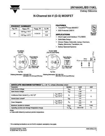
2N7000KL/BS170KL Vishay Siliconix N-Channel 60-V (D-S) MOSFET FEATURES PRODUCT SUMMARY TrenchFET Power MOSFET VDS (V) rDS(on) ( ) VGS(th) (V) ID (A) Pb-free ESD Protected 2000 V Available 2 at VGS = 10 V 0.47 60 1.0 to 2.5 RoHS* APPLICATIONS COMPLIANT 4 at VGS = 4.5 V 0.33 Direct Logic-Level Interface TTL/CMOS Solid-State Relays Drivers Relays,... See More ⇒
2n7002k.pdf
2N7002K Vishay Siliconix N-Channel 60-V (D-S) MOSFET FEATURES PRODUCT SUMMARY Halogen-free According to IEC 61249-2-21 VDS (V) RDS(on) ( )ID (mA) Definition 2 at VGS = 10 V 60 300 Low On-Resistance 2 Low Threshold 2 V (typ.) Low Input Capacitance 25 pF Fast Switching Speed 25 ns Low Input and Output Leakage TrenchFET Power MOSFET ... See More ⇒
2n7000 2n7002 vq1000j-p bs170.pdf

2N7000/2N7002, VQ1000J/P, BS170 Vishay Siliconix N-Channel 60-V (D-S) MOSFET PRODUCT SUMMARY Part Number V(BR)DSS Min (V) rDS(on) Max (W) VGS(th) (V) ID (A) 5 @ VGS = 10 V 0.8 to 3 0.2 2N7000 2N7002 7.5 @ VGS = 10 V 1 to 2.5 0.115 60 VQ1000J 5.5 @ VGS = 10 V 0.8 to 2.5 0.225 VQ1000P 5.5 @ VGS = 10 V 0.8 to 2.5 0.225 BS170 5 @ VGS = 10 V 0.8 to 3 0.5 FEATURES BENEFITS APPLICATIONS D... See More ⇒
2n7000 2n7002 vq1000j vq1000p bs170.pdf
2N7000/2N7002, VQ1000J/P, BS170 Vishay Siliconix N-Channel 60-V (D-S) MOSFET PRODUCT SUMMARY Part Number V(BR)DSS Min (V) rDS(on) Max (W) VGS(th) (V) ID (A) 5 @ VGS = 10 V 0.8 to 3 0.2 2N7000 2N7002 7.5 @ VGS = 10 V 1 to 2.5 0.115 60 VQ1000J 5.5 @ VGS = 10 V 0.8 to 2.5 0.225 VQ1000P 5.5 @ VGS = 10 V 0.8 to 2.5 0.225 BS170 5 @ VGS = 10 V 0.8 to 3 0.5 FEATURES BENEFITS APPLICATIONS D... See More ⇒
2n7002dw.pdf
2N7002DW DUAL N-CHANNEL ENHANCEMENT MODE FIELD EFFECT TRANSISTOR Features Mechanical Data Dual N-Channel MOSFET Case SOT-363 Low On-Resistance Case Material Molded Plastic. Green Molding Compound. UL Flammability Classification Rating 94V-0 Low Gate Threshold Voltage Moisture Sensitivity Level 1 per J-STD-020 Low Input Capacitance Termina... See More ⇒
2n7002.pdf
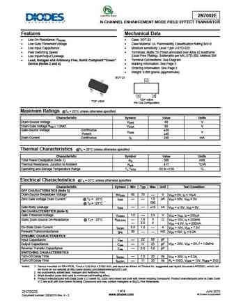
2N7002 N-CHANNEL ENHANCEMENT MODE FIELD EFFECT TRANSISTOR Features Mechanical Data Low On-Resistance Case SOT-23 Low Gate Threshold Voltage Case Material Molded Plastic, Green Molding Compound. UL Flammability Classification Rating 94V-0 Low Input Capacitance Moisture Sensitivity Level 1 per J-STD-020 Fast Switching Speed Terminals Matte... See More ⇒
2n7002aq.pdf
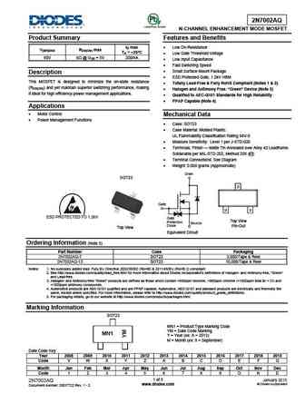
2N7002AQ N-CHANNEL ENHANCEMENT MODE MOSFET Product Summary Features and Benefits ID max Low On-Resistance V(BR)DSS RDS(ON) max TA = +25 C Low Gate Threshold Voltage 60V 6 @ VGS = 5V 200mA Low Input Capacitance Fast Switching Speed Small Surface Mount Package Description ESD Protected Gate, 1.2kV HBM This MOSFET is designed to minimize the on-s... See More ⇒
2n7002-7-f 2n7002-7.pdf
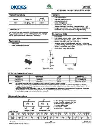
2N7002 N-CHANNEL ENHANCEMENT MODE MOSFET Product Summary Features Low On-Resistance ID max V(BR)DSS RDS(ON) max Low Gate Threshold Voltage TA = 25 C Low Input Capacitance 60V 7.5 @ VGS = 5V 210mA Fast Switching Speed Small Surface Mount Package Totally Lead-Free & Fully RoHS Compliant (Notes 1 & 2) Halogen and Antimony Free. Green Dev... See More ⇒
2n7002e.pdf
2N7002E N-CHANNEL ENHANCEMENT MODE FIELD EFFECT TRANSISTOR Features Mechanical Data Low On-Resistance RDS(ON) Case SOT-23 Low Gate Threshold Voltage Case Material UL Flammability Classification Rating 94V-0 Low Input Capacitance Moisture sensitivity Level 1 per J-STD-020 Fast Switching Speed Terminals Matte Tin Finish annealed over Alloy 42 leadfra... See More ⇒
2n7002vc-vac.pdf
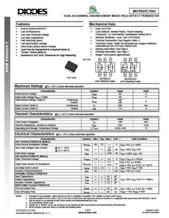
2N7002VC/VAC DUAL N-CHANNEL ENHANCEMENT MODE FIELD EFFECT TRANSISTOR Features Mechanical Data Dual N-Channel MOSFET Case SOT-563 Low On-Resistance Case Material Molded Plastic, Green Molding Compound. UL Flammability Classification Rating 94V-0 Low Gate Threshold Voltage Moisture Sensitivity Level 1 per J-STD-020C Low Input Capacitance T... See More ⇒
2n7002w.pdf
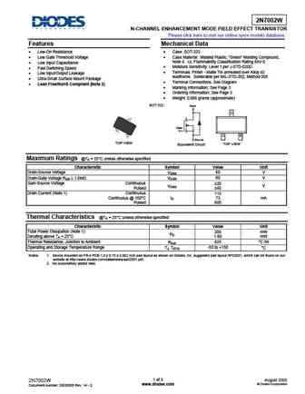
2N7002W N-CHANNEL ENHANCEMENT MODE FIELD EFFECT TRANSISTOR Please click here to visit our online spice models database. Features Mechanical Data Low-On Resistance Case SOT-323 Low Gate Threshold Voltage Case Material Molded Plastic, "Green" Molding Compound, Note 4. UL Flammability Classification Rating 94V-0 Low Input Capacitance Moisture Sensitivity Le... See More ⇒
2n7002k.pdf
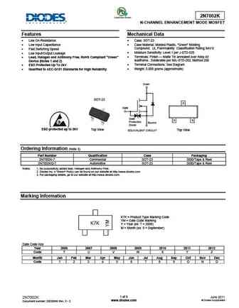
2N7002K N-CHANNEL ENHANCEMENT MODE MOSFET Features Mechanical Data Low On-Resistance Case SOT-23 Low Input Capacitance Case Material Molded Plastic, Green Molding Compound. UL Flammability Classification Rating 94V-0 Fast Switching Speed Moisture Sensitivity Level 1 per J-STD-020 Low Input/Output Leakage Terminals Finish Matte Tin an... See More ⇒
2n7002a.pdf
2N7002A N-CHANNEL ENHANCEMENT MODE FIELD EFFECT TRANSISTOR Please click here to visit our online spice models database. Features Mechanical Data N-Channel MOSFET Case SOT-23 Low On-Resistance Case Material Molded Plastic. UL Flammability Classification Rating 94V-0 Low Gate Threshold Voltage Moisture Sensitivity Level 1 per J-STD-020D Low Input Ca... See More ⇒
2n7002h.pdf
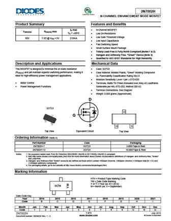
2N7002H N-CHANNEL ENHANCEMENT MODE MOSFET Product Summary Features and Benefits N-Channel MOSFET ID max V(BR)DSS RDS(ON) max TA = +25 C Low On-Resistance Low Gate Threshold Voltage 60V 7.5 @ VGS = 5V 210mA Low Input Capacitance Fast Switching Speed Small Surface Mount Package Totally Lead-Free & Fully RoHS Compliant (Notes 1 & 2) H... See More ⇒
2n7002t.pdf
2N7002T N-CHANNEL ENHANCEMENT MODE FIELD EFFECT TRANSISTOR Features Mechanical Data Low On-Resistance Case SOT523 Low Gate Threshold Voltage Case Material Molded Plastic. Green Molding Compound. UL Flammability Classification Rating 94V-0 Low Input Capacitance Moisture Sensitivity Level 1 per J-STD-020D Fast Switching Speed Terminals Sol... See More ⇒
2n7002vc 2n7002vac.pdf
2N7002VC/VAC DUAL N-CHANNEL ENHANCEMENT MODE MOSFET Features Mechanical Data Dual N-Channel MOSFET Case SOT563 Low On-Resistance Case Material Molded Plastic, Green Molding Compound. UL Flammability Classification Rating 94V-0 Low Gate Threshold Voltage Moisture Sensitivity Level 1 per J-STD-020 Low Input Capacitance Terminal Connection... See More ⇒
2n7002dw.pdf
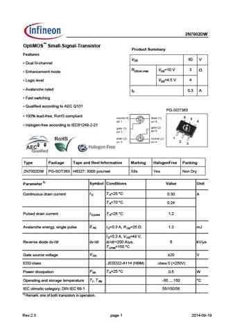
2N7002DW OptiMOS Small-Signal-Transistor Product Summary Features VDS 60 V Dual N-channel RDS(on),max VGS=10 V 3 W Enhancement mode Logic level VGS=4.5 V 4 Avalanche rated ID 0.3 A Fast switching Qualified according to AEC Q101 PG-SOT363 100% lead-free; RoHS compliant 6 5 4 Halogen-free according to IEC61249-2-21 1 2 3 Type ... See More ⇒
2n7002dw.pdf
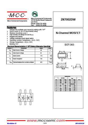
MCC Micro Commercial Components TM 2N7002DW 20736 Marilla Street Chatsworth Micro Commercial Components CA 91311 Phone (818) 701-4933 Fax (818) 701-4939 Features Halogen free available upon request by adding suffix "-HF" Epoxy meets UL 94 V-0 flammability rating Moisture Sensitivity Level 1 N-Channel MOSFET High density cell design for low RDS(ON) Rugged and r... See More ⇒
2n7002.pdf
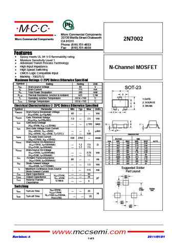
MCC Micro Commercial Components TM 20736 Marilla Street Chatsworth Micro Commercial Components 2N7002 CA 91311 Phone (818) 701-4933 Fax (818) 701-4939 Features Epoxy meets UL 94 V-0 flammability rating Moisture Sensitivity Level 1 Advanced Trench Process Technology High Input Impedance N-Channel MOSFET High Speed Switching CMOS Logic Compatible Input ... See More ⇒
2n7002w.pdf
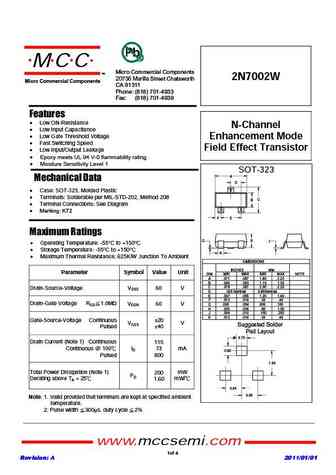
MCC TM Micro Commercial Components 20736 Marilla Street Chatsworth 2N7002W Micro Commercial Components CA 91311 Phone (818) 701-4933 Fax (818) 701-4939 Features Low ON-Resistance N-Channel Low Input Capacitance Low Gate Threshold Voltage Enhancement Mode Fast Switching Speed Field Effect Transistor Low Input/Output Leakage Epoxy meets UL 94 V-0 flamma... See More ⇒
2n7002k-tp.pdf
MCC TM Micro Commercial Components 20736 Marilla Street Chatsworth Micro Commercial Components 2N7002K CA 91311 Phone (818) 701-4933 Fax (818) 701-4939 Features Epoxy meets UL 94 V-0 flammability rating Moisture Sensitivity Level 1 High density cell design for low RDS(ON) Voltage controlled small signal switch N-Channel MOSFET Rugged and reliable Hig... See More ⇒
2n7002a.pdf
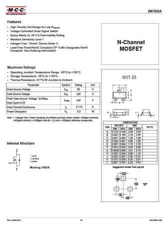
2N7002A Features High Density Cell Design for Low RDS(ON) Voltage Controlled Small Signal Switch Epoxy Meets UL 94 V-0 Flammability Rating Moisture Sensitivity Level 1 N-Channel Halogen Free. Green Device (Note 1) Lead Free Finish/RoHS Compliant ("P" Suffix Designates RoHS MOSFET Compliant. See Ordering Information) Maximum Ratings Operating Junct... See More ⇒
2n7002w-tp.pdf

MCC TM Micro Commercial Components 20736 Marilla Street Chatsworth 2N7002W Micro Commercial Components CA 91311 Phone (818) 701-4933 Fax (818) 701-4939 Features Low ON-Resistance N-Channel Low Input Capacitance Low Gate Threshold Voltage Enhancement Mode Fast Switching Speed Field Effect Transistor Low Input/Output Leakage Epoxy meets UL 94 V-0 flamma... See More ⇒
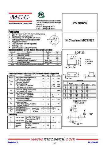
2n7002ka.pdf
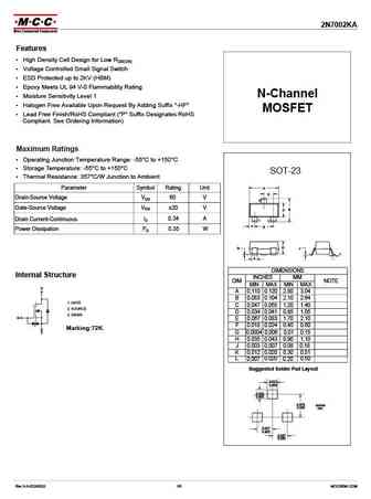
2N7002KA Features High Density Cell Design for Low RDS(ON) Voltage Controlled Small Signal Switch ESD Protected up to 2KV (HBM) Epoxy Meets UL 94 V-0 Flammability Rating N-Channel Moisture Sensitivity Level 1 Halogen Free Available Upon Request By Adding Suffix "-HF" MOSFET Lead Free Finish/RoHS Compliant ("P" Suffix Designates RoHS Compliant. See Ordering... See More ⇒
2n7002kwa.pdf
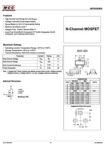
Features High Density Cell Design for Low RDS(ON) Voltage Controlled Small Signal Switch Epoxy Meets UL 94 V-0 Flammability Rating Moisture Sensitivity Level 1 Halogen Free. Green Device (Note 1) Lead Free Finish/RoHS Compliant ("P" Suffix Designates RoHS Compliant. See Ordering Information) Maximum Ratings Operating Junct... See More ⇒
2n7002dw.pdf

Is Now Part of To learn more about ON Semiconductor, please visit our website at www.onsemi.com Please note As part of the Fairchild Semiconductor integration, some of the Fairchild orderable part numbers will need to change in order to meet ON Semiconductor s system requirements. Since the ON Semiconductor product management systems do not have the ability to manage part nomenclatur... See More ⇒
2n7002kw.pdf
2N7002KW N-Channel Enhancement Mode Field Effect Transistor Features www.onsemi.com Low On-Resistance Low Gate Threshold Voltage D Low Input Capacitance Fast Switching Speed S Low Input/Output Leakage G Ultra-Small Surface Mount Package SC-70 3 LEAD These Devices are Pb-Free and are RoHS Compliant CASE 419AB ESD HBM = 1000 V as per JESD22 A114 a... See More ⇒
2n7000 2n7002 nds7002a.pdf
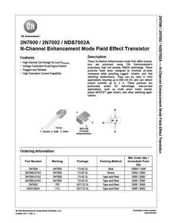
2N7000 / 2N7002 / NDS7002A N-Channel Enhancement Mode Field Effect Transistor Description Features These N-channel enhancement mode field effect transis- High Density Cell Design for Low RDS(ON) tors are produced using ON Semiconductor's Voltage Controlled Small Signal Switch proprietary, high cell density, DMOS technology. These Rugged and Reliable products have been de... See More ⇒
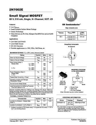
2n7002e.pdf
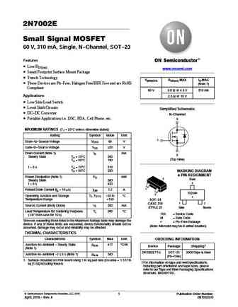
2N7002E Small Signal MOSFET 60 V, 310 mA, Single, N-Channel, SOT-23 Features Low RDS(on) www.onsemi.com Small Footprint Surface Mount Package Trench Technology V(BR)DSS RDS(on) MAX ID MAX These Devices are Pb-Free, Halogen Free/BFR Free and are RoHS (Note 1) Compliant 60 V 3.0 W @ 4.5 V 310 mA Applications 2.5 W @ 10 V Low Side Load Switch Level Shift Circ... See More ⇒
2v7002k 2n7002k.pdf
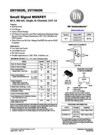
2N7002K, 2V7002K Small Signal MOSFET 60 V, 380 mA, Single, N-Channel, SOT-23 Features ESD Protected Low RDS(on) www.onsemi.com Surface Mount Package 2V Prefix for Automotive and Other Applications Requiring Unique V(BR)DSS RDS(on) MAX ID MAX Site and Control Change Requirements; AEC-Q101 Qualified and 1.6 W @ 10 V PPAP Capable 60 V 380 mA 2.5 W @ 4.5 V These D... See More ⇒
2n7002e 2.pdf
2N7002E Small Signal MOSFET 60 V, 310 mA, Single, N-Channel, SOT-23 Features Low RDS(on) http //onsemi.com Small Footprint Surface Mount Package Trench Technology V(BR)DSS RDS(on) MAX ID MAX These Devices are Pb-Free, Halogen Free/BFR Free and are RoHS (Note 1) Compliant 60 V 3.0 W @ 4.5 V 310 mA Applications 2.5 W @ 10 V Low Side Load Switch Level Shift C... See More ⇒
2n7002t.pdf
Is Now Part of To learn more about ON Semiconductor, please visit our website at www.onsemi.com Please note As part of the Fairchild Semiconductor integration, some of the Fairchild orderable part numbers will need to change in order to meet ON Semiconductor s system requirements. Since the ON Semiconductor product management systems do not have the ability to manage part nomenclatur... See More ⇒
2n7002l.pdf
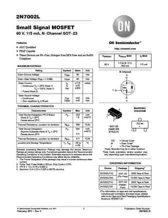
2N7002L Small Signal MOSFET 60 V, 115 mA, N-Channel SOT-23 Features AEC Qualified http //onsemi.com PPAP Capable These Devices are Pb-Free, Halogen Free/BFR Free and are RoHS V(BR)DSS RDS(on) MAX ID MAX Compliant 7.5 W @ 10 V, 60 V 115 mA 500 mA MAXIMUM RATINGS Rating Symbol Value Unit N-Channel Drain-Source Voltage VDSS 60 Vdc 3 Drain-Gate Voltage (RGS = 1.0 MW) V... See More ⇒
2n7002k 2v7002k.pdf
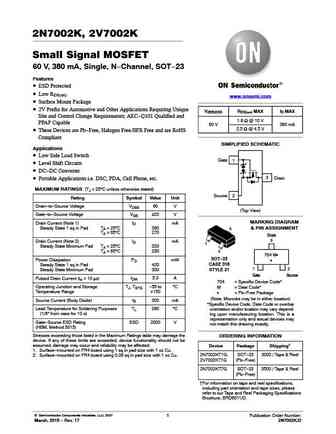
2N7002K, 2V7002K Small Signal MOSFET 60 V, 380 mA, Single, N-Channel, SOT-23 Features ESD Protected Low RDS(on) www.onsemi.com Surface Mount Package 2V Prefix for Automotive and Other Applications Requiring Unique V(BR)DSS RDS(on) MAX ID MAX Site and Control Change Requirements; AEC-Q101 Qualified and 1.6 W @ 10 V PPAP Capable 60 V 380 mA 2.5 W @ 4.5 V These D... See More ⇒
2n7002l 2v7002l.pdf
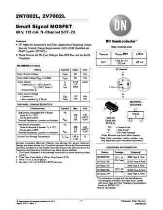
2N7002L, 2V7002L Small Signal MOSFET 60 V, 115 mA, N-Channel SOT-23 Features 2V Prefix for Automotive and Other Applications Requiring Unique http //onsemi.com Site and Control Change Requirements; AEC-Q101 Qualified and PPAP Capable (2V7002L) V(BR)DSS RDS(on) MAX ID MAX These Devices are Pb-Free, Halogen Free/BFR Free and are RoHS Compliant 7.5 W @ 10 V, 60 V 115 mA 500 mA... See More ⇒
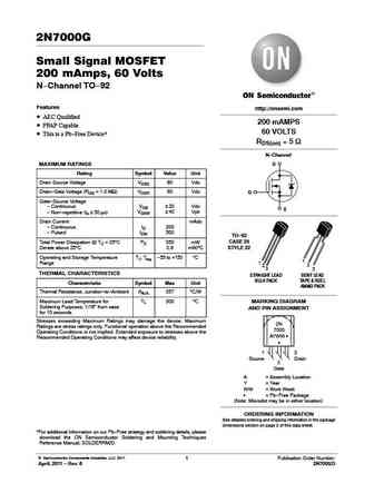
2n7000g 2n7000rlra 2n7000rlrag 2n7000rlrmg 2n7000rlrpg.pdf
2N7000G Small Signal MOSFET 200 mAmps, 60 Volts N-Channel TO-92 Features http //onsemi.com AEC Qualified 200 mAMPS PPAP Capable 60 VOLTS This is a Pb-Free Device* RDS(on) = 5 W N-Channel MAXIMUM RATINGS D Rating Symbol Value Unit Drain Source Voltage VDSS 60 Vdc Drain-Gate Voltage (RGS = 1.0 MW) VDGR 60 Vdc G Gate-Source Voltage - Continuous VGS 20 Vdc S - No... See More ⇒
2n7002kt1g.pdf
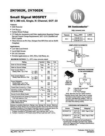
2N7002K, 2V7002K Small Signal MOSFET 60 V, 380 mA, Single, N-Channel, SOT-23 Features ESD Protected Low RDS(on) http //onsemi.com Surface Mount Package 2V Prefix for Automotive and Other Applications Requiring Unique V(BR)DSS RDS(on) MAX ID MAX Site and Control Change Requirements; AEC-Q101 Qualified and 1.6 W @ 10 V PPAP Capable 60 V 380 mA 2.5 W @ 4.5 V Thes... See More ⇒
2n7002w 2v7002w.pdf

2N7002W, 2V7002W Small Signal MOSFET 60 V, 340 mA, Single, N-Channel, SC-70 Features ESD Protected Low RDS(on) www.onsemi.com Small Footprint Surface Mount Package 2V Prefix for Automotive and Other Applications Requiring Unique V(BR)DSS RDS(on) MAX ID MAX Site and Control Change Requirements; AEC-Q101 Qualified and (Note 1) PPAP Capable 1.6 W @ 10 V These Devi... See More ⇒
2v7002w 2n7002w.pdf
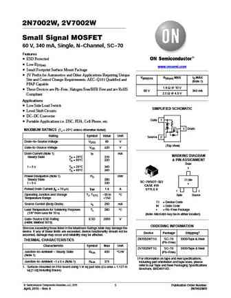
2N7002W, 2V7002W Small Signal MOSFET 60 V, 340 mA, Single, N-Channel, SC-70 Features ESD Protected Low RDS(on) www.onsemi.com Small Footprint Surface Mount Package 2V Prefix for Automotive and Other Applications Requiring Unique V(BR)DSS RDS(on) MAX ID MAX Site and Control Change Requirements; AEC-Q101 Qualified and (Note 1) PPAP Capable 1.6 W @ 10 V These Devi... See More ⇒
2n7000g.pdf

2N7000G Small Signal MOSFET 200 mAmps, 60 Volts N-Channel TO-92 Features http //onsemi.com AEC Qualified 200 mAMPS PPAP Capable 60 VOLTS This is a Pb-Free Device* RDS(on) = 5 W N-Channel MAXIMUM RATINGS D Rating Symbol Value Unit Drain Source Voltage VDSS 60 Vdc Drain-Gate Voltage (RGS = 1.0 MW) VDGR 60 Vdc G Gate-Source Voltage - Continuous VGS 20 Vdc S - No... See More ⇒
2v7002l 2n7002l.pdf
2N7002L, 2V7002L Small Signal MOSFET 60 V, 115 mA, N-Channel SOT-23 Features 2V Prefix for Automotive and Other Applications Requiring Site and http //onsemi.com Change Controls AEC Qualified - 2V7002L V(BR)DSS RDS(on) MAX ID MAX PPAP Capable - 2V7002L These Devices are Pb-Free, Halogen Free/BFR Free and are RoHS 7.5 W @ 10 V, 60 V 115 mA Compliant 500 mA N-Channel... See More ⇒
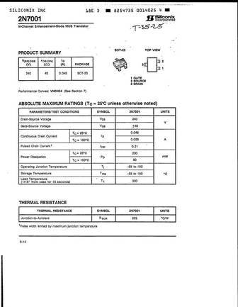
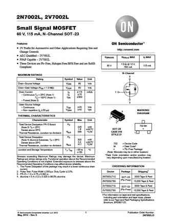
2n7007.pdf
2N7007 N-Channel Enhancement-Mode Vertical DMOS FET Ordering Information Order Number / Package BVDSS /RDS(ON) ID(ON) BVDGS (max) (min) TO-92 240V 45 150mA 2N7007 Features Advanced DMOS Technology These enhancement-mode (normally-off) transistors utilize a Free from secondary breakdown vertical DMOS structure and Supertex s well-proven silicon-gate Low power drive requirement... See More ⇒
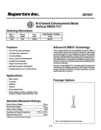
2n7008.pdf
2N7008 N-Channel Enhancement-Mode Vertical DMOS FETs Features General Description The Supertex 2N7008 is an enhancement-mode (normally- Free from secondary breakdown off) transistor that utilizes a vertical DMOS structure Low power drive requirement and Supertex s well-proven silicon-gate manufacturing Ease of paralleling process. This combination produces a device wit... See More ⇒
2n7002dw.pdf
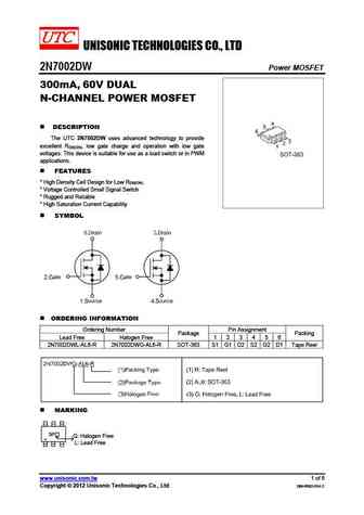
UNISONIC TECHNOLOGIES CO., LTD 2N7002DW Power MOSFET 300mA, 60V DUAL N-CHANNEL POWER MOSFET DESCRIPTION The UTC 2N7002DW uses advanced technology to provide excellent RDS(ON), low gate charge and operation with low gate voltages. This device is suitable for use as a load switch or in PWM applications. FEATURES * High Density Cell Design for Low R . DS(ON) * Voltage Co... See More ⇒
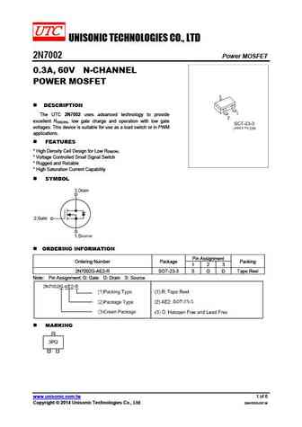
2n7002.pdf
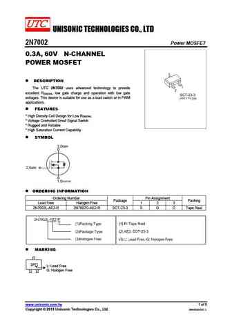
UNISONIC TECHNOLOGIES CO., LTD 2N7002 Power MOSFET 0.3A, 60V N-CHANNEL POWER MOSFET DESCRIPTION The UTC 2N7002 uses advanced technology to provide excellent RDS(ON), low gate charge and operation with low gate voltages. This device is suitable for use as a load switch or in PWM applications. FEATURES * High Density Cell Design for Low R . DS(ON) * Voltage Controlled S... See More ⇒
2n7000z.pdf
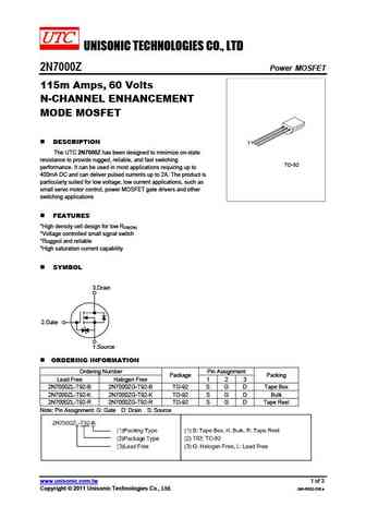
UNISONIC TECHNOLOGIES CO., LTD 2N7000Z Power MOSFET 115m Amps, 60 Volts N-CHANNEL ENHANCEMENT MODE MOSFET DESCRIPTION 1 The UTC 2N7000Z has been designed to minimize on-state resistance to provide rugged, reliable, and fast switching TO-92 performance. It can be used in most applications requiring up to 400mA DC and can deliver pulsed currents up to 2A. The product is p... See More ⇒
2n7000.pdf
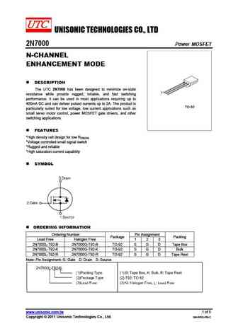
UNISONIC TECHNOLOGIES CO., LTD 2N7000 Power MOSFET N-CHANNEL ENHANCEMENT MODE DESCRIPTION The UTC 2N7000 has been designed to minimize on-state 1 resistance while provide rugged, reliable, and fast switching performance. It can be used in most applications requiring up to 400mA DC and can deliver pulsed currents up to 2A. The product is TO-92 particularly suited for low vo... See More ⇒
2n7002kl-ae2-r 2n7002kg-ae2-r.pdf
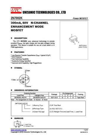
UNISONIC TECHNOLOGIES CO., LTD 2N7002K Power MOSFET 300mA, 60V N-CHANNEL ENHANCEMENT MODE MOSFET DESCRIPTION The UTC 2N7002K uses advanced technology to provide excellent RDS(ON), low gate charge and low gate voltages during operation. This device is suitable for use as a load switch or in PWM applications. FEATURES * Low Reverse Transfer Capacitance (CRSS = typica... See More ⇒
2n7002zt.pdf
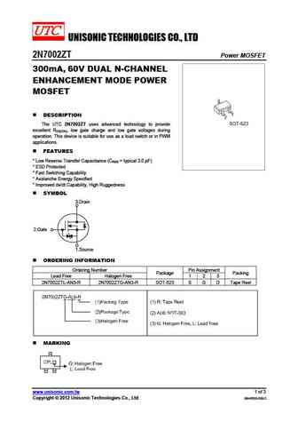
UNISONIC TECHNOLOGIES CO., LTD 2N7002ZT Power MOSFET 300mA, 60V DUAL N-CHANNEL ENHANCEMENT MODE POWER MOSFET DESCRIPTION The UTC 2N7002ZT uses advanced technology to provide excellent RDS(ON), low gate charge and low gate voltages during operation. This device is suitable for use as a load switch or in PWM applications. FEATURES * Low Reverse Transfer Capacitance (CRSS... See More ⇒
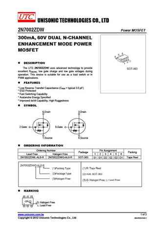
2n7002zdwg-al6-r.pdf
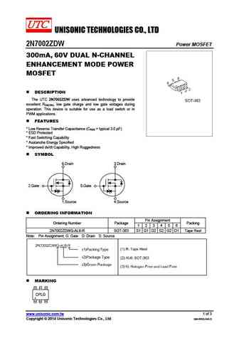
UNISONIC TECHNOLOGIES CO., LTD 2N7002ZDW Power MOSFET 300mA, 60V DUAL N-CHANNEL ENHANCEMENT MODE POWER MOSFET DESCRIPTION The UTC 2N7002ZDW uses advanced technology to provide excellent RDS(ON), low gate charge and low gate voltages during operation. This device is suitable for use as a load switch or in PWM applications. FEATURES * Low Reverse Transfer Capacitance... See More ⇒
2n7002w.pdf
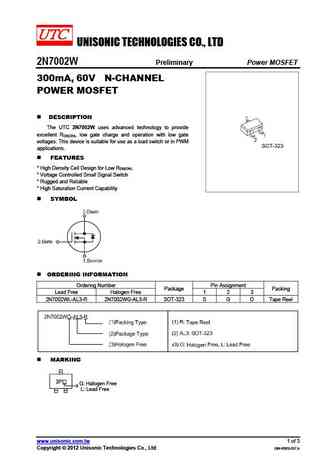
UNISONIC TECHNOLOGIES CO., LTD 2N7002W Preliminary Power MOSFET 300mA, 60V N-CHANNEL POWER MOSFET DESCRIPTION The UTC 2N7002W uses advanced technology to provide excellent RDS(ON), low gate charge and operation with low gate voltages. This device is suitable for use as a load switch or in PWM applications. FEATURES * High Density Cell Design for Low R . DS(ON) * Volta... See More ⇒
2n7002k.pdf
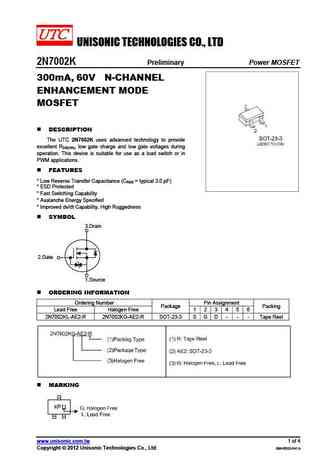
UNISONIC TECHNOLOGIES CO., LTD 2N7002K Preliminary Power MOSFET 300mA, 60V N-CHANNEL ENHANCEMENT MODE MOSFET DESCRIPTION The UTC 2N7002K uses advanced technology to provide excellent RDS(ON), low gate charge and low gate voltages during operation. This device is suitable for use as a load switch or in PWM applications. FEATURES * Low Reverse Transfer Capacitance (CRSS ... See More ⇒
2n7002zdw.pdf
UNISONIC TECHNOLOGIES CO., LTD 2N7002ZDW Power MOSFET 300mA, 60V DUAL N-CHANNEL ENHANCEMENT MODE POWER MOSFET DESCRIPTION The UTC 2N7002ZDW uses advanced technology to provide excellent RDS(ON), low gate charge and low gate voltages during operation. This device is suitable for use as a load switch or in PWM applications. FEATURES * Low Reverse Transfer Capacitance (CR... See More ⇒
2n7002g-ae2-r.pdf
UNISONIC TECHNOLOGIES CO., LTD 2N7002 Power MOSFET 0.3A, 60V N-CHANNEL POWER MOSFET DESCRIPTION The UTC 2N7002 uses advanced technology to provide excellent RDS(ON), low gate charge and operation with low gate voltages. This device is suitable for use as a load switch or in PWM applications. FEATURES * High Density Cell Design for Low R . DS(ON) * Voltage Controll... See More ⇒
2n7002t.pdf
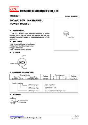
UNISONIC TECHNOLOGIES CO., LTD 2N7002T Power MOSFET 300mA, 60V N-CHANNEL POWER MOSFET DESCRIPTION The UTC 2N7002T uses advanced technology to provide excellent RDS(ON), low gate charge and operation with low gate voltages. This device is suitable for use as a load switch or in PWM applications. FEATURES * High Density Cell Design for Low R . DS(ON) * Voltage Contr... See More ⇒
2n7002ll.pdf
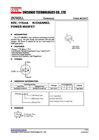
UNISONIC TECHNOLOGIES CO., LTD 2N7002LL Preliminary Power MOSFET 60V, 115mA N-CHANNEL POWER MOSFET DESCRIPTION 3 The UTC 2N7002LL uses advanced technology to provide excellent RDS(ON), low gate charge and operation with low gate 1 voltages. This device is suitable for use as a load switch or in 2 PWM applications. FEATURES SOT-23-3 (JEDEC TO-236) * RDS(ON) = 7.5 ... See More ⇒
2n7002z.pdf
UNISONIC TECHNOLOGIES CO., LTD 2N7002Z Power MOSFET 300mA, 60V N-CHANNEL ENHANCEMENT MODE POWER MOSFET DESCRIPTION The UTC 2N7002Z uses advanced technology to provide excellent RDS(ON), low gate charge and operation with low gate voltages. This device is suitable for use as a load switch or in PWM applications. FEATURES * RDS(ON) ... See More ⇒
2n7002b.pdf
2N7002B N-Channel Enhancement Mode MOSFET High Speed Switching Application Features ESD rating 2000V (HBM) Low On-Resistance RDS(on) ... See More ⇒
2n7000k.pdf
2N7000K N-Channel Enhancement Mode MOSFET High Speed Switching Application Features ESD rating 1000V (HBM) Low On-Resistance RDS(on) ... See More ⇒
2n7002k.pdf
2N7002K N-Channel Enhancement Mode MOSFET High Speed Switching Application COLLECTOR Features 3 ESD rating 1000V (HBM) 3 Low On-Resistance R ... See More ⇒
2n7002ku.pdf
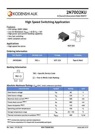
2N7002KU N-Channel Enhancement Mode MOSFET High Speed Switching Application Features ESD rating 2000V (HBM) Low On-Resistance R ... See More ⇒
2n7002ks6.pdf
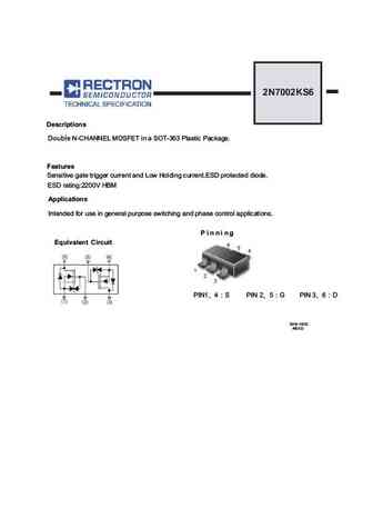
2N7002KS6 Descriptions N-CHANNEL MOSFET in a SOT-363 Plastic Package. Features Sensitive gate trigger current and Low Holding current.ESD protected diode. ESD rating 2200V HBM Applications Intended for use in general purpose switching and phase control applications. Pi nni ng Equivalent Circuit PIN1 4 S PIN 2 5 G PIN 3 6 D 2018-10/33 REV D Absolute Maximum Ratings(Ta=25 ... See More ⇒
2n7002dcsm.pdf
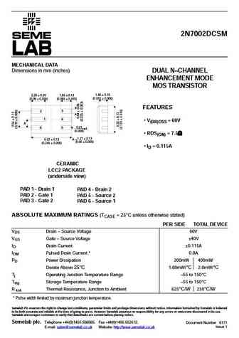
2N7002DCSM MECHANICAL DATA Dimensions in mm (inches) DUAL N CHANNEL ENHANCEMENT MODE MOS TRANSISTOR 1.40 0.15 2.29 0.20 1.65 0.13 (0.055 0.006) (0.09 0.008) (0.065 0.005) FEATURES 2 3 1 4 V(BR)DSS = 60V A 0.23 6 5 rad. (0.009) RDS(ON) = 7.5 6.22 0.13 A = 1.27 0.13 (0.05 0.005) (0.245 0.005) ID = 0.115A CERAMIC LCC2 PA... See More ⇒
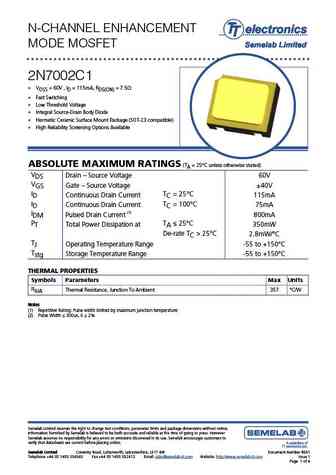
2n7002c1c 2n7002c1d.pdf
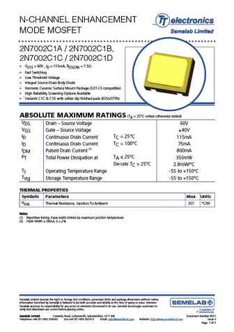
N-CHANNEL ENHANCEMENT MODE MOSFET 2N7002C1A / 2N7002C1B, 2N7002C1C / 2N7002C1D VDSS = 60V , ID = 115mA, RDS(ON) = 7.5 Fast Switching Low Threshold Voltage Integral Source-Drain Body Diode Hermetic Ceramic Surface Mount Package (SOT-23 compatible) High Reliability Screening Options Available Variants C1C & C1D with solder dip finished pads (63Sn... See More ⇒
2n7002csm.pdf
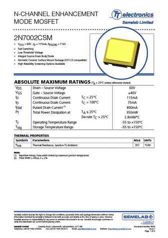
N-CHANNEL ENHANCEMENT MODE MOSFET 2N7002CSM VDSS = 60V , ID = 115mA, RDS(ON) = 7.5 Fast Switching Low Threshold Voltage Integral Source-Drain Body Diode Hermetic Ceramic Surface Mount Package (SOT-23 compatible) High Reliability Screening Options Available ABSOLUTE MAXIMUM RATINGS (TA = 25 C unless otherwise stated) VDS Drain Source Voltage ... See More ⇒
2n7002c1a 2n7002c1b.pdf
N-CHANNEL ENHANCEMENT MODE MOSFET 2N7002C1 VDSS = 60V , ID = 115mA, RDS(ON) = 7.5 Fast Switching Low Threshold Voltage Integral Source-Drain Body Diode Hermetic Ceramic Surface Mount Package (SOT-23 compatible) High Reliability Screening Options Available ABSOLUTE MAXIMUM RATINGS (TA = 25 C unless otherwise stated) VDS Drain Source Voltage 6... See More ⇒
2n7000csm.pdf
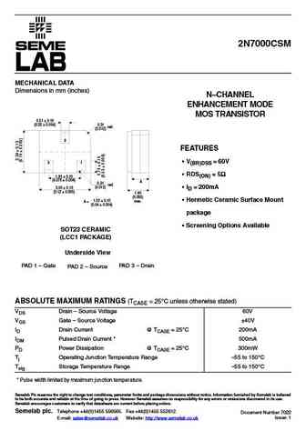
2N7000CSM MECHANICAL DATA Dimensions in mm (inches) N CHANNEL ENHANCEMENT MODE MOS TRANSISTOR 0.51 0.10 (0.02 0.004) 0.31 rad. (0.012) 3 FEATURES V(BR)DSS = 60V 21 RDS(ON) = 5 1.91 0.10 (0.075 0.004) A 0.31 rad. (0.012) 3.05 0.13 ID = 200mA (0.12 0.005) 1.40 (0.055) 1.02 0.10 Hermetic Ceramic Surface Mount max. A = (0.04 ... See More ⇒
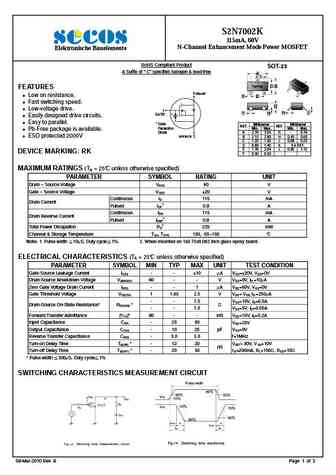
2n7002kw.pdf
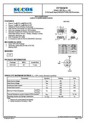
2N7002KW 115mA , 60V, RDS(ON) 4 N-Ch Small Signal MOSFET with ESD Protection Elektronische Bauelemente RoHS Compliant Product A suffix of -C specifies halogen & lead-free FEATURES SOT-323 RDS(ON), VGS@10V, IDS@500mA=3 RDS(ON), VGS@4.5V, IDS@200mA=4 A Advanced Trench Process Technology L High Density Cell Design For Ultra Low On-Resistance ... See More ⇒
2n7000.pdf
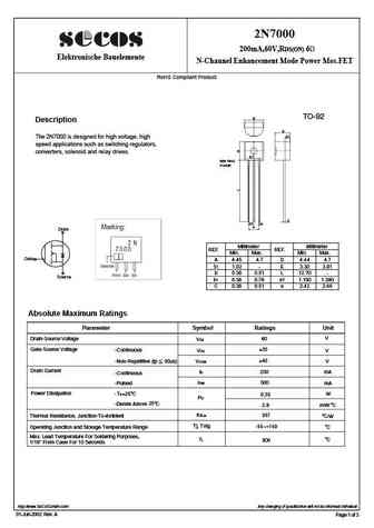
2N7000 200mA,60V,RDS(ON) 6 Elektronische Bauelemente N-Channel Enhancement Mode Power Mos.FET RoHS Compliant Product TO-92 D Description E S1 The 2N7000 is designed for high voltage, high speed applications such as switching regulators, converters, solenoid and relay drives. b1 SEATING PLANE C e1 b e Drain Millimeter Millimeter REF. REF. Min. Max. Min. Max. Gat... See More ⇒
s2n7002w.pdf
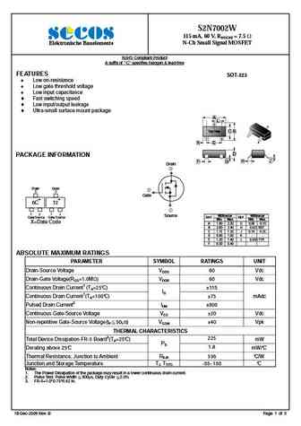
S2N7002W 115 mA, 60 V, RDS(ON) = 7.5 N-Ch Small Signal MOSFET Elektronische Bauelemente RoHS Compliant Product A suffix of -C specifies halogen & lead-free FEATURES SOT-323 Low on-resistance Low gate threshold voltage Low input capacitance Fast switching speed Low input/output leakage Ultra-small surface mount package A L 3 3 Top... See More ⇒
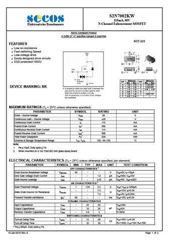
2n7002k.pdf
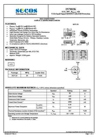
2N7002K 0.3A , 60V , RDS(ON) 4 N-Ch Small Signal MOSFET with ESD Protection Elektronische Bauelemente RoHS Compliant Product A suffix of -C specifies halogen & lead-free FEATURES SOT-23 RDS(ON), VGS@10V, IDS@500mA=3 RDS(ON), VGS@4.5V, IDS@200mA=4 A L Advanced Trench Process Technology 3 3 High Density Cell Design For Ultra Low On-Resista... See More ⇒
s2n7002.pdf
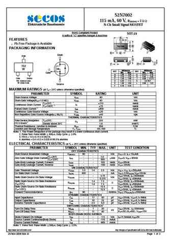
S2N7002 115 mA, 60 V, RDS(ON) = 7.5 Elektronische Bauelemente N-Ch Small Signal MOSFET RoHS Compliant Product SOT-23 A suffix of -C specifies halogen & lead-free A L FEATURES 3 3 Pb-Free Package is Available Top View C B PACKAGING INFORMATION 1 1 2 2 K E Drain Drain 3 3 D H J F G 702 W 1 Millimeter Millimeter REF. REF. Min. Max. Min. ... See More ⇒
2n7002t.pdf
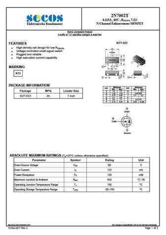
2N7002T 0.115A , 60V , RDS(ON) 7.2 N-Channel Enhancement MOSFET Elektronische Bauelemente RoHS Compliant Product A suffix of -C specifies halogen & lead-free SOT-523 FEATURES High density cell design for low RDS(ON). A Voltage controlled small signal switch. M Rugged and reliable. 3 3 High saturation current capability. Top View C B 1 1 2 ... See More ⇒
s2n7002k.pdf
S2N7002K 115mA, 60V N-Channel Enhancement Mode Power MOSFET Elektronische Bauelemente RoHS Compliant Product SOT-23 A Suffix of -C specifies halogen & lead-free A L 3 3 Top View C B FEATURES 1 1 2 3 DRAIN 2 Low on resistance. K E Fast switching speed. D Low-voltage drive. 1 H J F G GATE * Easily designed drive circuits. Easy to parallel. ... See More ⇒
s2n7002dw.pdf
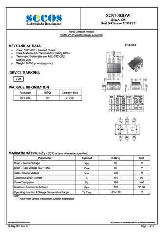
S2N7002DW 115mA, 60V Dual N-Channel MOSFET Elektronische Bauelemente RoHS Compliant Product A Suffix of -C specifies halogen & lead-free SOT-363 MECHANICAL DATA Case SOT-363 Molded Plastic. Case Material-UL Flammability Rating 94V-0 Terminals Solderable per MIL-STD-202, Method 208 Weight 0.006 grams(approx.) DEVICE MARKING 702 PACKAGE INF... See More ⇒
s2n7002kw.pdf
S2N7002KW 115mA, 60V N-Channel Enhancement MOSFET Elektronische Bauelemente RoHS Compliant Product A Suffix of -C specifies halogen & lead-free SOT-323 FEATURES Low on-resistance Fast switching Speed A L Low-voltage drive 3 3 Easily designed drive circuits Top View C B 1 1 2 ESD protected 1500V 2 K E D H J F G Millimeter Millimeter REF. REF. ... See More ⇒
2n7002kdw.pdf
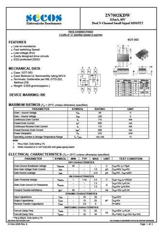
2N7002KDW 115mA, 60V Dual N-Channel Small Signal MOSFET Elektronische Bauelemente RoHS Compliant Product A Suffix of -C specifies halogen & lead-free SOT-363 FEATURES A Low on-resistance E L Fast switching Speed 6 5 4 Low-voltage drive Easily designed drive circuits B ESD protected 2000V 1 2 3 F C H 6 5 4 MECHANICAL DATA J D2 G1 S1 D ... See More ⇒
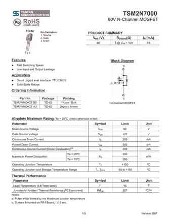
tsm2n7000kct.pdf
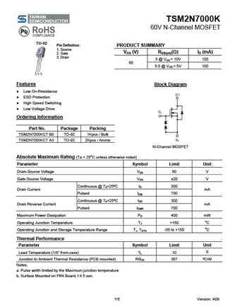
TSM2N7000K 60V N-Channel MOSFET TO-92 Pin Definition PRODUCT SUMMARY 1. Source VDS (V) RDS(on)( ) ID (mA) 2. Gate 3. Drain 5 @ VGS = 10V 100 60 5.5 @ VGS = 5V 100 Features Block Diagram Low On-Resistance ESD Protection High Speed Switching Low Voltage Drive Ordering Information Part No. Package Packing TSM2N7000KCT B0 TO-92 1Kpcs / Bulk ... See More ⇒
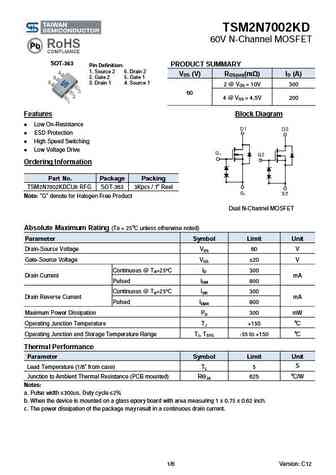
tsm2n7002kdcu6.pdf
TSM2N7002KD 60V N-Channel MOSFET SOT-363 PRODUCT SUMMARY Pin Definition 1. Source 2 6. Drain 2 VDS (V) RDS(on)(m ) ID (A) 2. Gate 2 5. Gate 1 3. Drain 1 4. Source 1 2 @ VGS = 10V 300 60 4 @ VGS = 4.5V 200 Features Block Diagram Low On-Resistance ESD Protection High Speed Switching Low Voltage Drive Ordering Information Part No. Package Pa... See More ⇒
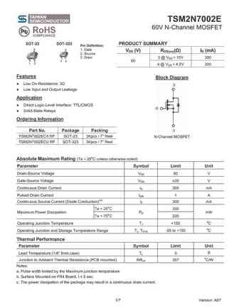
tsm2n7002kcx.pdf
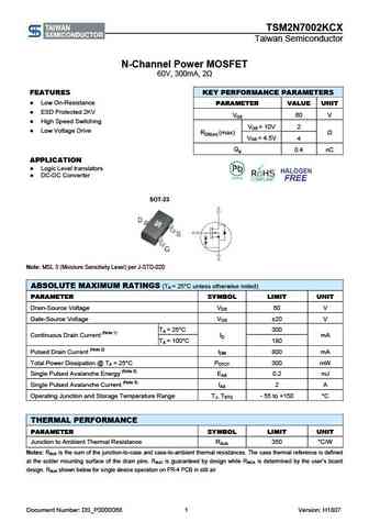
TSM2N7002KCX Taiwan Semiconductor N-Channel Power MOSFET 60V, 300mA, 2 FEATURES KEY PERFORMANCE PARAMETERS Low On-Resistance PARAMETER VALUE UNIT ESD Protected 2KV VDS 60 V High Speed Switching VGS = 10V 2 Low Voltage Drive RDS(on) (max) VGS = 4.5V 4 Qg 0.4 nC APPLICATION Logic Level translators DC-DC Converter SOT-23 Note... See More ⇒
tsm2n7002kcu tsm2n7002kcx.pdf
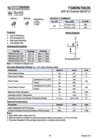
TSM2N7002K 60V N-Channel MOSFET SOT-23 SOT-323 PRODUCT SUMMARY Pin Definition 1. Gate VDS (V) RDS(on)( ) ID (mA) 2. Source 3. Drain 2 @ VGS = 10V 300 60 4 @ VGS = 4.5V 200 Features Block Diagram Low On-Resistance ESD Protected 2KV High Speed Switching Low Voltage Drive Ordering Information Part No. Package Packing TSM2N7002KCX RF SOT-23 ... See More ⇒
2n7002dw.pdf
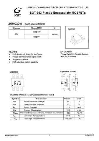
JIANGSU CHANGJIANG ELECTRONICS TECHNOLOGY CO., LTD SOT-363 Plastic-Encapsulate MOSFETs 2N7002DW Dual N-channel MOSFET ID V(BR)DSS RDS(on)MAX SOT-363 5 @10V 60V 115mA @5V 7 APPLICATION FEATURE High density cell design for low RDS(ON) Load Switch for Portable Devices DC/DC Converter Voltage controlled small signal switch Rugged and reliable High ... See More ⇒
2n7002.pdf
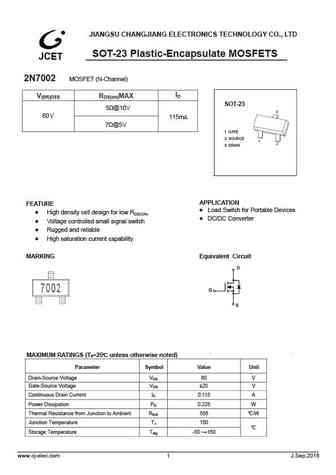
JIANGSU CHANGJIANG ELECTRONICS TECHNOLOGY CO., LTD SOT-23 Plastic-Encapsulate MOSFETS 2N7002 MOSFET (N-Channel) ID V(BR)DSS RDS(on)MAX SOT-23 5 @10V 3 60V 115mA 7 @5V 1. GATE 2. SOURCE 1 2 3. DRAIN APPLICATION FEATURE Load Switch for Portable Devices High density cell design for low RDS(ON) DC/DC Converter Voltage controlled small signal sw... See More ⇒
2n7002kw.pdf
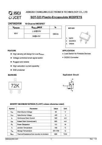
JIANGSU CHANGJING ELECTRONICS TECHNOLOGY CO., LTD SOT-323 Plastic-Encapsulate MOSFETS 2N7002KW N-Channel MOSFET ID V(BR)DSS RDS(on)MAX SOT-323 2.5 3 1. GATE 2. SOURCE 1 2 3. DRAIN FEATURE APPLICATION High density cell design for Low RDS(on) Voltage controlled sm... See More ⇒
2n7000.pdf
JIANGSU CHANGJIANG ELECTRONICS TECHNOLOGY CO., LTD TO-92 Plastic-Encapsulate MOSFETS TO-92 2N7000 MOSFET (N-Channel) 1. SOURCE FEATURES High density cell design for low RDS(ON) 2. GATE Voltage controlled small signal switch 3. DRAIN Rugged and reliable High saturation current capability MAXIMUM RATINGS (Ta=25 unless otherwise noted) Parameter Symbol Value ... See More ⇒
2n7002w.pdf
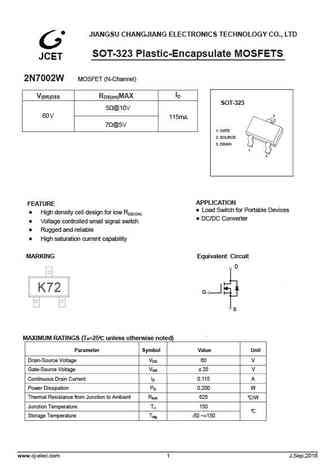
2 JIANGSU CHANGJIANG ELECTRONICS TECHNOLOGY CO., LTD SOT-323 Plastic-Encapsulate MOSFETS 2N7002W MOSFET (N-Channel) ID V(BR)DSS RDS(on)MAX SOT-323 5 @10V 3 60V 115mA 7 @5V 1. GATE 2. SOURCE 3. DRAIN 1 2 APPLICATION FEATURE Load Switch for Portable Devices High density cell design for low RDS(ON) DC/DC Converter Voltage controlled small sig... See More ⇒
2n7002k.pdf
JIANGSU CHANGJIANG ELECTRONICS TECHNOLOGY CO., LTD SOT-23 Plastic-Encapsulate MOSFETs 2N7002K N-channel MOSFET SOT-23 FEATURES z High density cell design for Low RDS on z Voltage controlled small signal switch 1. GATE 2. SOURCE z Rugged and reliable 3. DRAIN z High saturation current capability z ESD protected up to 2KV Marking 72K Equivalent circuit MOSFET ... See More ⇒
2n7002v.pdf
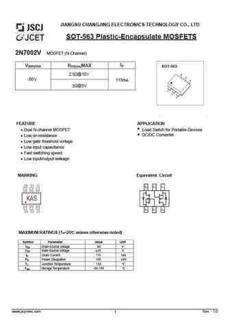
JIANGSU CHANGJING ELECTRONICS TECHNOLOGY CO., LTD SOT-563 Plastic-Encapsulate MOSFETS 2N7002V MOSFET (N-Channel) ID V(BR)DSS RDS(on)MAX SOT-563 6 2.5 @10V 5 60V 4 115mA 3 @5V 1 2 3 FEATURE APPLICATION Dual N-channel MOSFET Load Switch for Portable Devices DC/DC Converter Low on-resistance Low gate threshold voltage Low input capacitance ... See More ⇒
2n7002t.pdf
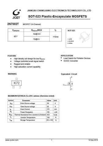
JIANGSU CHANGJIANG ELECTRONICS TECHNOLOGY CO., LTD SOT-523 Plastic-Encapsulate MOSFETS 2N7002T MOSFET (N-Channel) ID V(BR)DSS RDS(on)MAX SOT-523 5 @10V 60V 115mA 1. GATE 7 @5V 2. SOURCE 3. DRAIN APPLICATION FEATURE Load Switch for Portable Devices High density cell design for low RDS(ON) DC/DC Converter Voltage controlled small signal switch ... See More ⇒
2n7002kdw.pdf
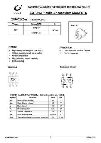
JIANGSU CHANGJIANG ELECTRONICS TECHNOLOGY CO., LTD SOT-363 Plastic-Encapsulate MOSFETS 2N7002KDW N-channel MOSFET ID V(BR)DSS RDS(on)MAX SOT-363 5 @10V 6 60V 5 340mA 4 5.3 @4.5V 1 2 3 FEATURE APPLICATION z High density cell design for Low RDS on Load Switch for Portable Devices z Voltage controlled small signal switch DC/DC Converter z Rugged ... See More ⇒
2n7002x.pdf
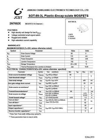
JIANGSU CHANGJIANG ELECTRONICS TECHNOLOGY CO., LTD SOT-89-3L Plastic-Encap sulate MOSFETS SOT-89-3L 2N7002X MOSFET( N-Channel ) 1 1 2 FEA TURES 2 3 3 High density cell design for low RDS(on) 1.GATE Voltage controlled small signal switch 2. DRAIN Rugged and reliable 3. SOURCE High saturation current capability MARKING K72 MAXIMUM RATINGS (Ta=25 ... See More ⇒
2n7002.pdf
2N7002 SEMICONDUCTOR N CHANNEL ENHANCEMENT MODE TECHNICAL DATA FIELD EFFECT TRANSISTOR INTERFACE AND SWITCHING APPLICATION. FEATURES E L B L High density cell design for low RDS(ON). DIM MILLIMETERS Voltage controlled small signal switch. _ + A 2.93 0.20 B 1.30+0.20/-0.15 Rugged and reliable. C 1.30 MAX 2 3 High saturation current capablity. D 0.45+0.15/-0.05 E 2.40+0.30/... See More ⇒
2n7000.pdf
2N7000 SEMICONDUCTOR N CHANNEL ENHANCEMENT MODE TECHNICAL DATA FIELD EFFECT TRANSISTOR INTERFACE AND SWITCHING APPLICATION. B C FEATURES High density cell design for low RDS(ON). Voltage controlled small signal switch. Rugged and reliable. N DIM MILLIMETERS High saturation current capablity. A 4.70 MAX E K B 4.80 MAX G C 3.70 MAX D D 0.45 E 1.00 F 1.27 G 0.85 MAXIMUM RA... See More ⇒
2n7000k.pdf
2N7000K SEMICONDUCTOR N Channel MOSFET TECHNICAL DATA ESD Protected 2000V INTERFACE AND SWITCHING APPLICATION. B C FEATURES ESD Protected 2000V. High density cell design for low RDS(ON). Voltage controlled small signal switch. N DIM MILLIMETERS Rugged and reliable. A 4.70 MAX E K B 4.80 MAX High saturation current capablity. G C 3.70 MAX D D 0.45 E 1.00 F 1.27 G 0.85 H ... See More ⇒
2n7002k.pdf
2N7002K SEMICONDUCTOR N Channel MOSFET TECHNICAL DATA ESD Protected 2000V INTERFACE AND SWITCHING APPLICATION. FEATURES E L B L ESD Protected 2000V. DIM MILLIMETERS High density cell design for low RDS(ON). _ A + 2.93 0.20 B 1.30+0.20/-0.15 Voltage controlled small signal switch. C 1.30 MAX 2 3 Rugged and reliable. D 0.45+0.15/-0.05 E 2.40+0.30/-0.20 High saturation curr... See More ⇒
2n7002a.pdf
2N7002A SEMICONDUCTOR N CHANNEL ENHANCEMENT MODE TECHNICAL DATA FIELD EFFECT TRANSISTOR INTERFACE AND SWITCHING APPLICATION. FEATURES E L B L High density cell design for low RDS(ON). DIM MILLIMETERS Voltage controolled small signal switch. _ A + 2.93 0.20 B 1.30+0.20/-0.15 Rugged and reliable. C 1.30 MAX 2 3 High saturation current capablity. D 0.45+0.15/-0.05 E 2.40+0.3... See More ⇒
2n7002ka.pdf
2N7002KA SEMICONDUCTOR N Channel MOSFET TECHNICAL DATA ESD Protected 2000V INTERFACE AND SWITCHING APPLICATION. FEATURES E L B L ESD Protected 2000V. DIM MILLIMETERS _ + High density cell design for low RDS(ON). A 2.93 0.20 B 1.30+0.20/-0.15 Voltage controlled small signal switch. C 1.30 MAX 2 3 D 0.40+0.15/-0.05 Rugged and reliable. E 2.40+0.30/-0.20 1 G 1.90 ... See More ⇒
2n7000a.pdf
2N7000A SEMICONDUCTOR N CHANNEL ENHANCEMENT MODE TECHNICAL DATA FIELD EFFECT TRANSISTOR INTERFACE AND SWITCHING APPLICATION. B C FEATURES High density cell design for low RDS(ON). Voltage controolled small signal switch. Rugged and reliable. N DIM MILLIMETERS High saturation current capablity. A 4.70 MAX E K B 4.80 MAX G C 3.70 MAX D D 0.45 E 1.00 F 1.27 G 0.85 ... See More ⇒
2n7002.pdf
2N7002 60V N-Channel Enhancement Mode MOSFET Feature SOT-23 60V/0.2A, RDS(ON) = 7.5 (MAX) @VGS = 10V. Id = 0.5A RDS(ON) = 7.5 (MAX) @VGS = 5V . Id = 0.05A Super High dense cell design for extremely low RDS(ON) . Reliable and Rugged. SOT-23 for Surface Mount Package. 1. GATE 2. SOURCE 3. DRAIN Applications Power Management in Desktop Computer or DC/DC Conver... See More ⇒
2n7002.pdf
2N7002 Mosfet (N-Channel) SOT-23 1. GATE 2. SOURCE 3. DRAIN Features High density cell design for low RDS(ON) Voltage controlled small signal switch Rugged and reliable High saturation current capability Marking 7002 Dimensions in inches and (millimeters) MAXIMUM RATINGS (TA=25 unless otherwise noted) Symbol Parameter Value Units VDS Drain-Source voltage 60 V ... See More ⇒
2n7000.pdf
2N7000 Mosfet (N-Channel) TO-92 1. SOURCE 2. GATE 3. DRAIN Features High density cell design for low RDS(ON) Voltage controlled small signal switch Rugged and reliable High saturation current capability MAXIMUM RATINGS (TA=25 unless otherwise noted) Symbol Parameter Value Units VDS Drain-Source voltage 60 V Dimensions in inches and (millimeters) ID Drain Curr... See More ⇒
2n7002w.pdf
2N7002W Mosfet(N-Channel) SOT-323 1. GATE 2. SOURCE 3. DRAIN Features High density cell design for low RDS(ON) Voltage controlled small signal switch Rugged and reliable High saturation current capability Marking K72 Dimensions in inches and (millimeters) MAXIMUM RATINGS (TA=25 unless otherwise noted) Symbol Parameter Value Units VDS Drain-Source voltage 60 V... See More ⇒
2n7002dw.pdf
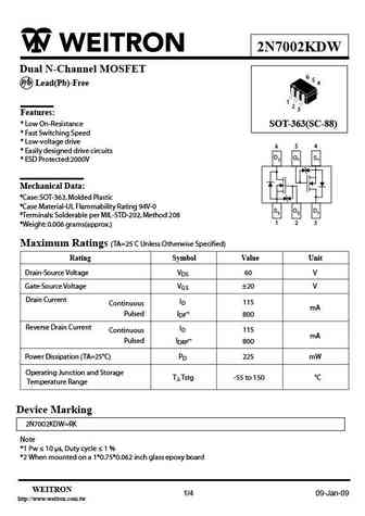
2N7002DW Dual N-Channel MOSFET 6 5 4 1 2 3 Features * We declare that the material of product are Halogen Free and SOT-363(SC-88) compliance with RoHS requirements. * ESD Protected 1000V 3 2 1 D2 G1 S1 S2 G2 D1 4 5 6 Maximum Ratings (TA=25 C Unless Otherwise Specified) Rating Symbol Value Unit Drain-Source Voltage VDS 60 V Drain-Gate Voltage RGS... See More ⇒
2n7002.pdf
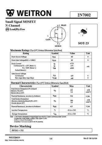
WEITRON 2N7002 Small Signal MOSFET 3 DRAIN N-Channel 3 P b Lead(Pb)-Free 1 2 1 GATE SOT-23 2 SOURCE Maximum Ratings (T =25 C Unless Otherwise Specified) A Rating Symbol Value Unit Drain Source Voltage VDSS 60 V Drain Gate Voltage(RGS = 1.0M ) VDGR 60 V 115 Drain Current ID Continuous TC = 25 C (Note 1.) 75 ID mA Con tinuous IDM 800 TC= 100 C (Note 1.) P... See More ⇒
2n7000.pdf
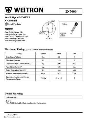
WEITRON 2N7000 Small Signal MOSFET N-Channel 3 DRAIN TO-92 Features 2 1 *Low On-Resistance 5 GATE 1. SOURCE 2 3 *Low Input Capacitance 60PF 2. GATE 3. DRAIN *Low Out put Capacitance 25PF 1 SOURCE *Low Threshole 1.4V(TYE) *Fast Switching Speed 10ns Maximum Ratings (TA=25 C Unless Otherwise Specified) Rating Symbol Value Unit Drain-Source Voltage VDS 60 V Gate-S... See More ⇒
2n7002w.pdf
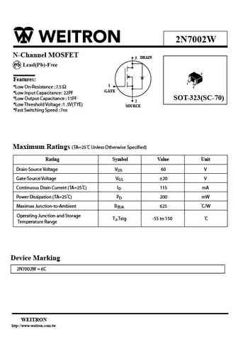
2N7002W N-Channel MOSFET 3 DRAIN 3 Features 1 1 2 *Low On-Resistance 7.5 GATE *Low Input Capacitance 22PF SOT-323(SC-70) *Low Output Capacitance 11PF 2 *Low Threshold Voltage 1 .5V(TYE) SOURCE *Fast Switching Speed 7ns Maximum Ratings (TA=25 C Unless Otherwise Specified) Rating Symbol Value Unit Drain-Source Voltage VDS 60 V Gate-Source Voltage VGS 20 V Conti... See More ⇒
2n7002k.pdf
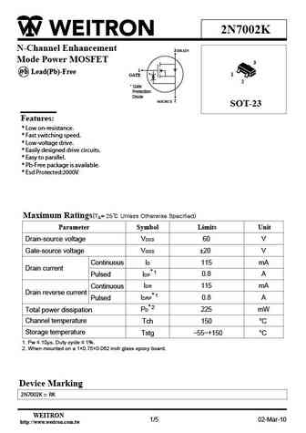
2N7002K N-Channel Enhancement 3 DRAIN Mode Power MOSFET 3 1 P b Lead(Pb)-Free 1 GATE * 2 * Gate Pretection Diode SOURCE 2 SOT-23 Features * Low on-resistance. * Fast switching speed. * Low-voltage drive. * Easily designed drive circuits. * Easy to parallel. * Pb-Free package is available. * Esd Protected 2000V Maximum Ratings(T = 25 Unless Otherwise Specified) A ... See More ⇒
2n7002t.pdf
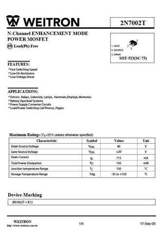
2N7002T N-Channel ENHANCEMENT MODE POWER MOSFET 3 1. GATE 1 P b Lead(Pb)-Free 2 2. SOURCE 3. DRAIN SOT-523(SC-75) FEATURES * Fast Switching Speed * Low On-Resistance * Low Voltage Driver APPLICATIONS * Drivers Relays, Solenoids, Lamps, Hammers,Displays, Memories * Battery Operated Systems * Power Supply Converter Circuits * Load/Power Switching Cell Phones, Pagers Maximu... See More ⇒
2n7002kdw.pdf
2N7002KDW Dual N-Channel MOSFET 6 5 P b Lead(Pb)-Free 4 1 2 3 Features * Low On-Resistance SOT-363(SC-88) * Fast Switching Speed * Low-voltage drive 6 5 4 * Easily designed drive circuits D2 G1 S1 * ESD Protected 2000V Mechanical Data *Case SOT-363, Molded Plastic *Case Material-UL Flammability Rating 94V-0 S2 G2 D1 *Terminals Solderable per MIL-STD-202, Method 208 1 2... See More ⇒
2n7002kt.pdf
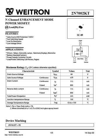
2N7002KT N-Channel ENHANCEMENT MODE POWER MOSFET 3 P b Lead(Pb)-Free 1 2 FEATURES SC-89 * Gate-Source ESD Protected 1500 V * Fast Switching Speed Drain * Low On-Resistance * Low Voltage Driver 3 APPLICATIONS * Drivers Relays, Solenoids, Lamps, Hammers,Displays, Memories * Battery Operated Systems * Power Supply Converter Circuits 1 (Top View) 2 * Load/Power Switching Ce... See More ⇒
2n7002lt1.pdf
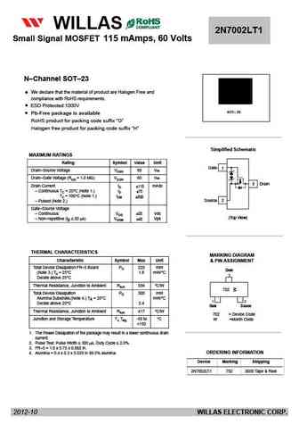
FM120-M WILLAS THRU 2N7002LT1 Small Signal MOSFET 115 mAmps, 60 Volts FM1200-M 1.0A SURFACE MOUNT SCHOTTKY BARRIER RECTIFIERS -20V- 200V SOD-123 PACKAGE Pb Free Product Package outline Features Batch process design, excellent power dissipation offers better reverse leakage current and thermal resistance. SOD-123H Low profile surface mounted application in order to ... See More ⇒
2n7002wt1.pdf
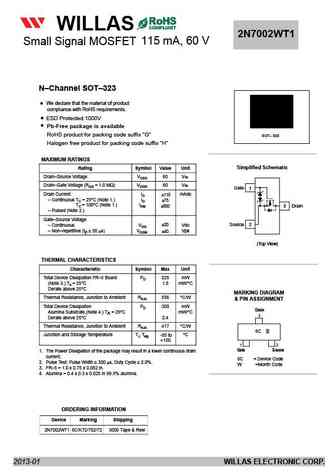
FM120-M WILLAS THRU 2N7002WT1 115 mA, 60 V Small Signal MOSFET FM1200-M 1.0A SURFACE MOUNT SCHOTTKY BARRIER RECTIFIERS -20V- 200V SOD-123 PACKAGE Pb Free Product Package outline Features Batch process design, excellent power dissipation offers better reverse leakage current and thermal resistance. SOD-123H Low profile surface mounted application in order to N Ch... See More ⇒
2n7002nt1.pdf
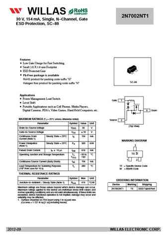
FM120-M WILLAS THRU 2N7002NT1 30 V, 154 mA, Single, N-Channel, Gate FM1200-M 1.0A SURFACE MOUNT SCHOTTKY BARRIER RECTIFIERS -20V- 200V ESD Protection, SC-89 SOD-123 PACKAGE Pb Free Product Package outline Features Batch process design, excellent power dissipation offers better reverse leakage current and thermal resistance. SOD-123H Low profile surface mounted appl... See More ⇒
2n7002t.pdf
FM120-M WILLAS THRU 2N7002T SOT-523 Plastic-Encapsulate MOSFETS FM1200-M 1.0A SURFACE MOUNT SCHOTTKY BARRIER RECTIFIERS -20V- 200V SOD-123 PACKAGE Pb Free Product Package outline Features Ba tch process design, excellent power dissipation offers better reverse leakage current and thermal resistance. SOD-123H MOSFET (N-Channel) nted application in order to Low prof... See More ⇒
2n7002elt1.pdf
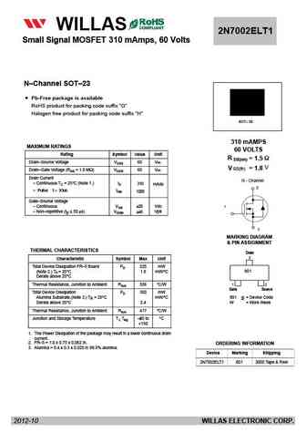
FM120-M WILLAS 2N7002ELT1 THRU Small Signal MOSFET 310 mAmps, 60 Volts FM1200-M 1.0A SURFACE MOUNT SCHOTTKY BARRIER RECTIFIERS -20V- 200V SOD-123 PACKAGE Pb Free Product Package outline Features Batch process design, excellent power dissipation offers better reverse leakage current and thermal resistance. SOD-123H Low profile surface mounte N Channel SOT 23d ap... See More ⇒
2n7002dw1t1.pdf
FM120-M WILLAS THRU 2N7002DW1T1 FM1200-M 1.0A SURFACE MOUNT SCHOTTKY BARRIER RECTIFIERS -20V- 200V Small Signal MOSFET 115 mAmps,60 Volts SOD-123 PACKAGE Pb Free Product Package outline Features Batch process design, excellent power dissipation offers N Channel SOT-363 better reverse leakage current and thermal resistance. SOD-123H Low profile surface mounted app... See More ⇒
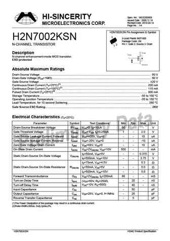
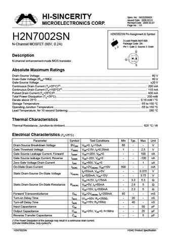
h2n7002ksn.pdf
Spec. No. MOS200809 HI-SINCERITY Issued Date 2008.11.18 Revised Date 2010.04.14 MICROELECTRONICS CORP. Page No. 1/4 H2N7002KSN Pin Assignment & Symbol 3 3-Lead Plastic SOT-323 H2N7002KSN Package Code SN Pin 1 Gate 2 Source 3 Drain N-CHANNEL TRANSISTOR 2 1 Description N-channel enhancement-mode MOS transistor. ESD protected Absolute Maximum Ratings Drai... See More ⇒
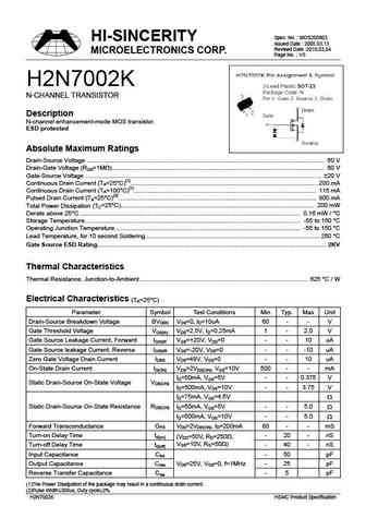
h2n7002k.pdf
Spec. No. MOS200803 HI-SINCERITY Issued Date 2005.03.13 Revised Date 2010,03,04 MICROELECTRONICS CORP. Page No. 1/5 H2N7002K N-CHANNEL TRANSISTOR Description N-channel enhancement-mode MOS transistor. ESD protected Absolute Maximum Ratings Drain-Source Voltage ............................................................................................................ See More ⇒
h2n7000.pdf
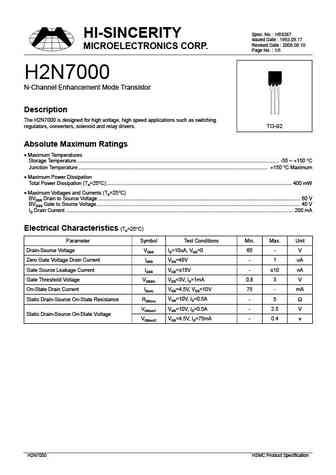
Spec. No. HE6267 HI-SINCERITY Issued Date 1993.09.17 Revised Date 2006.08.10 MICROELECTRONICS CORP. Page No. 1/5 H2N7000 N-Channel Enhancement Mode Transistor Description The H2N7000 is designed for high voltage, high speed applications such as switching regulators, converters, solenoid and relay drivers. TO-92 Absolute Maximum Ratings Maximum Temperatures Storage Temp... See More ⇒
h2n7002.pdf
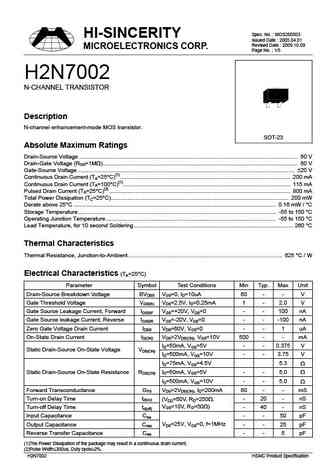
Spec. No. MOS200503 HI-SINCERITY Issued Date 2005.04.01 Revised Date 2009.10.09 MICROELECTRONICS CORP. Page No. 1/5 H2N7002 N-CHANNEL TRANSISTOR Description N-channel enhancement-mode MOS transistor. SOT-23 Absolute Maximum Ratings Drain-Source Voltage ................................................................................................................... See More ⇒
h2n7002sn.pdf
Spec. No. MOS200605 HI-SINCERITY Issued Date 2006.02.01 Revised Date 2006.02.07 MICROELECTRONICS CORP. Page No. 1/5 H2N7002SN Pin Assignment & Symbol H2N7002SN 3 3-Lead Plastic SOT-323 Package Code SN N-Channel MOSFET (60V, 0.2A) Pin 1 Gate 2 Source 3 Drain 2 1 D Description G N-channel enhancement-mode MOS transistor. S Absolute Maximum Ratings Drain-Source Vol... See More ⇒
ap2n7002k-hf.pdf
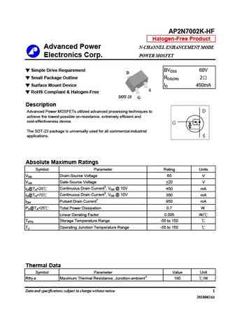
AP2N7002K-HF Halogen-Free Product Advanced Power N-CHANNEL ENHANCEMENT MODE Electronics Corp. POWER MOSFET Simple Drive Requirement BVDSS 60V D Small Package Outline RDS(ON) 2 Surface Mount Device ID 450mA S RoHS Compliant & Halogen-Free SOT-23 G Description D Advanced Power MOSFETs utilized advanced processing techniques to achieve the lowest possible on-resist... See More ⇒
ap2n7002ku.pdf
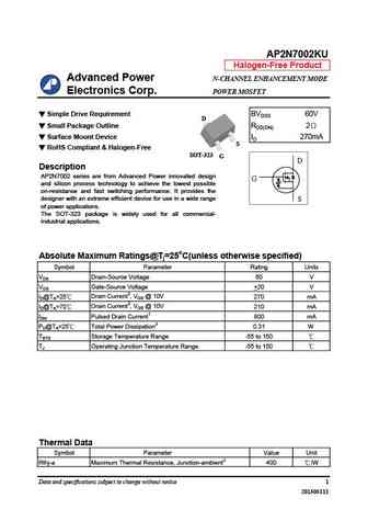
AP2N7002KU Halogen-Free Product Advanced Power N-CHANNEL ENHANCEMENT MODE Electronics Corp. POWER MOSFET Simple Drive Requirement BVDSS 60V D Small Package Outline RDS(ON) 2 Surface Mount Device ID 270mA S RoHS Compliant & Halogen-Free SOT-323 G D Description AP2N7002 series are from Advanced Power innovated design G and silicon process technology to achieve th... See More ⇒
2n7002k.pdf
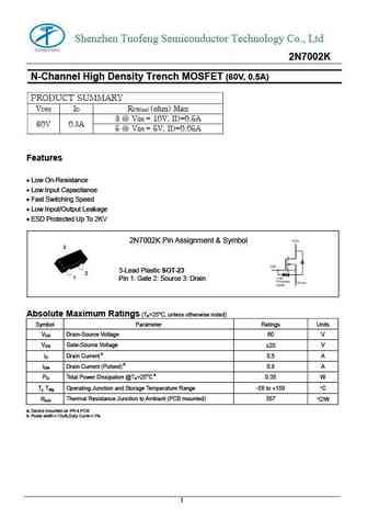
Shenzhen Tuofeng Semiconductor Technology Co., Ltd 2N7002K N-Channel High Density Trench MOSFET (60V, 0.5A) PRODUCT SUMMARY VDSS ID RDS(on) (ohm) Max 3 @ VGS = 10V, ID=0.5A 60V 0.5A 5 @ VGS = 5V, ID=0.05A Features Low On-Resistance Low Input Capacitance Fast Switching Speed Low Input/Output Leakage ESD Protected Up To 2KV 2N7002K Pin Assignment & Symbol... See More ⇒
pz2n7002m.pdf
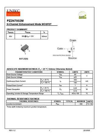
PZ2N7002M N-Channel Enhancement Mode MOSFET PRODUCT SUMMARY V(BR)DSS RDS(ON) ID 2 @VGS = 10V 60V 300mA SOT-23(S) ABSOLUTE MAXIMUM RATINGS (TA = 25 C Unless Otherwise Noted) PARAMETERS/TEST CONDITIONS SYMBOL LIMITS UNITS VDS Drain-Source Voltage 60 V VGS Gate-Source Voltage 25 TC = 25 C 300 ID Continuous Drain Current mA TC = 100 C 190 IDM 1 A Pulsed Drain C... See More ⇒
2n7002kb.pdf
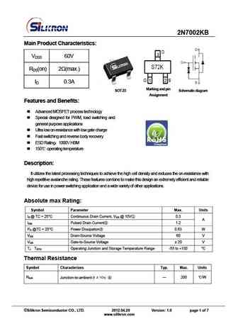
2N7002KB Main Product Characteristics VDSS 60V RDS(on) 2 (max.) ID 0.3A Marking and pin SOT-23 Schema t ic diag r am Assignment Features and Benefits Advanced MOSFET process technology Special designed for PWM, load switching and general purpose applications Ultra low on-resistance with low gate charge Fast switching and reverse body recovery ... See More ⇒
2n7002kg8.pdf
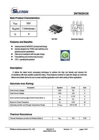
2N7002KG8 Main Product Characteristics VDSS 60V RDS(on) 7.5ohm(max.) ID A SOT-363 Sc he mat i c d ia gra m Features and Benefits Advanced trench MOSFET process technology Special designed for PWM, load switching and general purpose applications Ultra low on-resistance with low gate charge Fast switching and reverse body recovery 150 operating t... See More ⇒
2n7002 sot-23.pdf
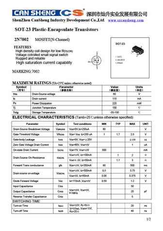
ShenZhen CanSheng Industry Development Co.,Ltd. www.szcansheng.com SOT-23 Plastic-Encapsulate Transistors 2N7002 MOSFET(N-Channel) FEATURES High density cell design for low RDS(ON) Voltage cotrolled small signal switch Rugged and reliable High saturation current capability MARKING 7002 MAXIMUM RATINGS (TA=25 unless otherwise noted... See More ⇒
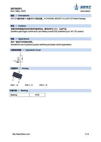
2n7002k.pdf
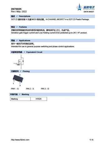
2N7002K Rev.I May.-2022 DATA SHEET / Descriptions SOT-23 N MOS N-CHANNEL MOSFET in a SOT-23 Plastic Package. / Features 2KV Sensitive gate trigger current and Low Holding current.ESD protected up to 2KV. HF product. / Applications ... See More ⇒
br2n7002lk2.pdf
BR2N7002LK2 Rev.C Oct.-2023 DATA SHEET / Descriptions SOT-23 N MOS N-CHANNEL MOSFET in a SOT-23 Plastic Package. / Features 2KV Sensitive gate trigger current and Low Holding current.ESD protected up to 2KV,HF Product. / Applications... See More ⇒
br2n7002ak2.pdf

BR2N7002AK2 Rev.D Oct.-2023 DATA SHEET / Descriptions SOT-23 N MOS N-CHANNEL MOSFET in a SOT-23 Plastic Package. / Features 2KV Sensitive gate trigger current and Low Holding current.ESD protected up to 2KV, HF Product. / Application... See More ⇒
st2n7000.pdf
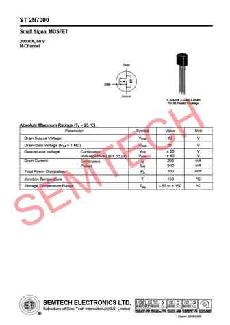
ST 2N7000 Small Signal MOSFET 200 mA, 60 V N-Channel Drain Gate Source 1. Source 2.Gate 3.Drain TO-92 Plastic Package O Absolute Maximum Ratings (Ta = 25 C) Parameter Symbol Value Unit Drain Source Voltage VDSS 60 V Drain-Gate Voltage (RGS = 1 M ) VDGR 60 V Gate-source Voltage Continuous VGS 20 V VGSM 40 V Non-repetitive ( tp 50 s) Drain Current Continuous... See More ⇒
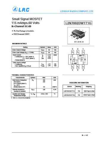
l2n7002dw1t1g s-l2n7002dw1t1g.pdf
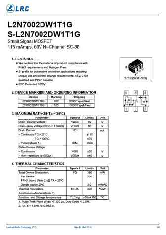
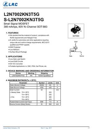
L2N7002DW1T1G S-L2N7002DW1T1G Small Signal MOSFET 115 mAmps, 60V N Channel SC-88 1. FEATURES We declare that the material of product compliance with RoHS requirements and Halogen Free. S- prefix for automotive and other applications requiring unique site and control change requirements; AEC-Q101 SC88(SOT-363) qualified and PPAP capable. ESD Protected 1000V 2. DE... See More ⇒
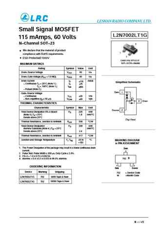
l2n7002klt1g.pdf
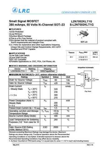
LESHAN RADIO COMPANY, LTD. Small Signal MOSFET L2N7002KLT1G 380 mAmps, 60 Volts N Channel SOT 23 S-L2N7002KLT1G FEATURES 3 1)ESD Protected 2)Low RDS(on) 1 3)Surface Mount Package 2 4)This is a Pb-Free Device 5)We declare that the material of product compliant with SOT 23 RoHS requirements and Halogen Free. 6) S- Prefix for Automotive and Other Applications Requiring Un... See More ⇒
l2n7002dmt1g.pdf
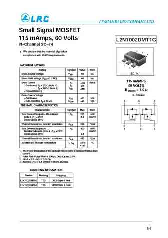
LESHAN RADIO COMPANY, LTD. Small Signal MOSFET 115 mAmps, 60 Volts L2N7002DMT1G N Channel SC 74 We declare that the material of product compliance with RoHS requirements. MAXIMUM RATINGS Rating Symbol Value Unit SC-74 Drain Source Voltage VDSS 60 Vdc Drain Gate Voltage (RGS = 1.0 M ) VDGR 60 Vdc 115 mAMPS Drain Current ID 115 mAdc Continuous TC = 25 C (Note 1... See More ⇒
l2n7002lt1g s-l2n7002lt1g.pdf
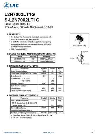
L2N7002LT1G S-L2N7002LT1G Small Signal MOSFET 115 mAmps, 60 Volts N Channel SOT-23 1. FEATURES We declare that the material of product compliance with RoHS requirements and Halogen Free. S- prefix for automotive and other applications requiring unique site and control change requirements; AEC-Q101 SOT23(TO-236) qualified and PPAP capable. ESD Protected 1000V 2. ... See More ⇒
l2n7002m3t5g s-l2n7002m3t5g.pdf
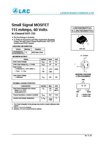
LESHAN RADIO COMPANY, LTD. Small Signal MOSFET L2N7002M3T5G 115 mAmps, 60 Volts S-L2N7002M3T5G N Channel SOT 723 3 Pb-Free Package is Available. S- Prefix for Automotive and Other Applications Requiring Unique Site and Control Change Requirements; AEC-Q101 Qualified and PPAP Capable. 2 1 ORDERING INFORMATION SOT-723 Device Marking Shipping L2N7002M3T5G 72 8000 Tap... See More ⇒
l2n7002sdw1t1g l2n7002sdw1t3g.pdf
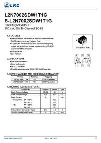
L2N7002SDW1T1G S-L2N7002SDW1T1G Small Signal MOSFET 380 mA, 60V N Channel SC-88 1. FEATURES We declare that the material of product compliance with RoHS requirements and Halogen Free. S- prefix for automotive and other applications requiring unique site and control change requirements; AEC-Q101 SC88(SOT-363) qualified and PPAP capable. ESD protected Low RDS... See More ⇒
l2n7002lt1g.pdf
LESHAN RADIO COMPANY, LTD. Small Signal MOSFET L2N7002LT1G 115 mAmps, 60 Volts N Channel SOT 23 3 We declare that the material of product 1 compliance with RoHS requirements. 2 ESD Protected 1000V CASE 318, STYLE 21 SOT 23 (TO 236AB) MAXIMUM RATINGS Rating Symbol Value Unit Drain Source Voltage VDSS 60 Vdc Drain Gate Voltage (RGS = 1.0 M ) VDGR 60 Vd... See More ⇒
l2n7002kdw1t1g l2n7002kdw1t3g.pdf
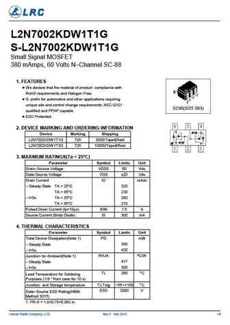
L2N7002KDW1T1G S-L2N7002KDW1T1G Small Signal MOSFET 380 mAmps, 60 Volts N Channel SC-88 1. FEATURES We declare that the material of product compliance with RoHS requirements and Halogen Free. S- prefix for automotive and other applications requiring unique site and control change requirements; AEC-Q101 SC88(SOT-363) qualified and PPAP capable. ESD Protected 2. D... See More ⇒
l2n7002wt1g.pdf
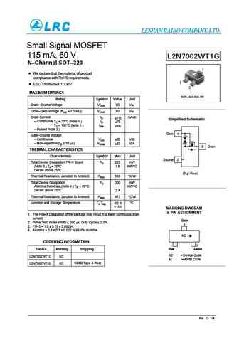
LESHAN RADIO COMPANY, LTD. Small Signal MOSFET 115 mA, 60 V L2N7002WT1G N Channel SOT 323 3 We declare that the material of product compliance with RoHS requirements. 1 ESD Protected 1000V 2 MAXIMUM RATINGS SOT 323 (SC-70) Rating Symbol Value Unit Drain Source Voltage VDSS 60 Vdc Drain Gate Voltage (RGS = 1.0 M ) VDGR 60 Vdc Drain Current ID 115 mAdc Sim... See More ⇒
l2n7002swt1g s-l2n7002swt1g.pdf

L2N7002SWT1G S-L2N7002SWT1G Small Signal MOSFET 380 mAmps, 60 Volts N Channel SC-70 1. FEATURES We declare that the material of product compliance with RoHS requirements and Halogen Free. S- prefix for automotive and other applications requiring unique site and control change requirements; AEC-Q101 SC70(SOT-323) qualified and PPAP capable. ESD protected Low R... See More ⇒
l2n7002slt1g l2n7002slt3g.pdf
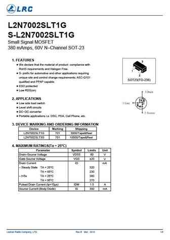
L2N7002SLT1G S-L2N7002SLT1G Small Signal MOSFET 380 mAmps, 60V N Channel SOT-23 1. FEATURES We declare that the material of product compliance with RoHS requirements and Halogen Free. S- prefix for automotive and other applications requiring unique site and control change requirements; AEC-Q101 SOT23(TO-236) qualified and PPAP capable. ESD protected Low RDS... See More ⇒
l2n7002dw1t1g.pdf
LESHAN RADIO COMPANY, LTD. Small Signal MOSFET 115 mAmps,60 Volts L2N7002DW1T1G N Channel SC-88 Pb-Free Package is Available. ESD Protected 1000V MAXIMUM RATINGS Rating Symbol Value Unit 3 2 1 Drain-Source Voltage VDSS 60 Vdc D2 G1 S1 Drain-Gate Voltage (RGS = 1.0 MW) VDGR 60 Vdc Drain Current ID 115 mAdc ID 75 - Continuous TC = 25 C (Note 1) IDM 800 - Continuo... See More ⇒
l2n7002flt1g.pdf
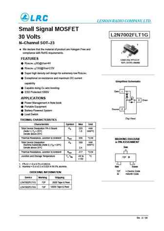
LESHAN RADIO COMPANY, LTD. Small Signal MOSFET L2N7002FLT1G 30 Volts N Channel SOT 23 3 We declare that the material of product are Halogen Free and compliance with RoHS requirements. 1 2 FEATURES CASE 318, STYLE 21 SOT 23 (TO 236AB) RDS(ON) 8 @VGS=4V RDS(ON) 13 @VGS=2.5V Super high density cell design for extremely low RDS(ON) Exce... See More ⇒
h2n7000.pdf
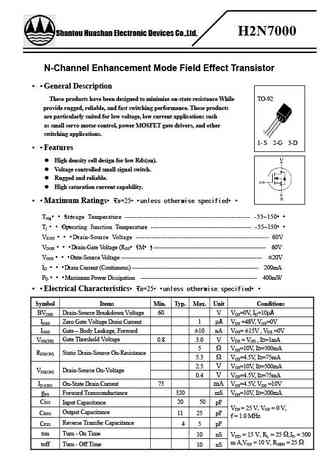
H2N7000 Shantou Huashan Electronic Devices Co.,Ltd. N-Channel Enhancement Mode Field Effect Transistor General Description These products have been designed to minimize on-state resistance While TO-92 provide rugged, reliable, and fast switching performance. These products are particularly suited for low voltage, low current applications such as small servo motor control, pow... See More ⇒
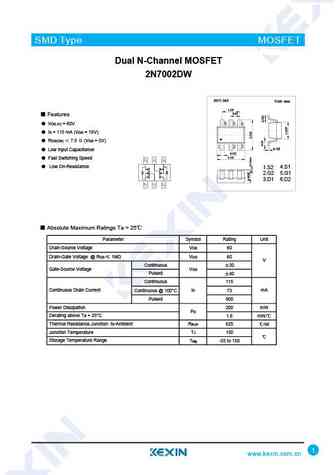
2n7002.pdf
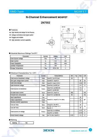
SMD Type MOSFET N-Channel Enhancement MOSFET 2N7002 SOT-23 Unit mm +0.1 2.9 -0.1 0.4+0.1 -0.1 Features 3 High density cell design for low RDS(ON) Voltage controlled small signal switch Rugged and reliable 1 2 High saturation current capability +0.1 +0.05 0.95 -0.1 0.1-0.01 +0.1 1.9-0.1 1.Base 1 GATE 2.Emitter 2 SOURCE 3.collector 3 DRAIN Absolute Maximum Ratings Ta=2... See More ⇒
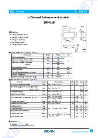
2n7002e.pdf
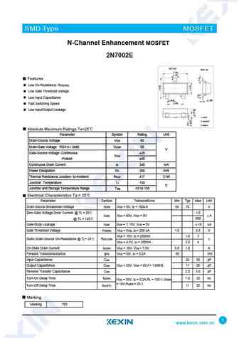
SMD Type MOSFET N-Channel Enhancement MOSFET 2N7002E SOT-23 Unit mm +0.1 2.9 -0.1 +0.1 0.4 -0.1 Features 3 Low On-Resistance RDS(ON) Low Gate Threshold Voltage 1 2 Low Input Capacitance +0.1 +0.05 0.95 -0.1 0.1 -0.01 +0.1 1.9 -0.1 Fast Switching Speed Low Input/Output Leakage 1.Base 1 GATE 2.Emitter 2 SOURCE 3 DRAIN Absolute Maximum Ratings Ta=25 Parameter Symbol Ra... See More ⇒
2n7002te.pdf
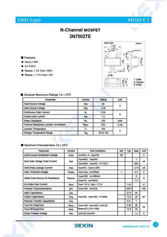
SMD Type MOSFET N-Channel MOSFET 2N7002TE SOT-523 Unit mm +0. 1 1.6 -0. 1 +0.1 1.0 -0.1 +0.05 0.2 -0.05 0.15 0.05 2 1 Features VDS (V) = 60V ID = 0.29 A 3 RDS(ON) 2 (VGS = 20V) 0.3 0.05 +0.1 0.5 -0.1 RDS(ON) 7.5 (VGS = 5V) 1. Gate 2. Source 3. Drain Absolute Maximum Ratings Ta = 25 Parameter Symbol Rating Unit Drain-Source ... See More ⇒
2n7002w.pdf
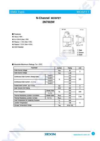
SMD Type MOSFET N-Channel MOSFET 2N7002W Features VDS (V) = 60V ID = 0.34 A (VGS = 10V) RDS(ON) 1.6 (VGS = 10V) RDS(ON) 2.5 (VGS = 4.5V) ESD Protected 1 Gate 2 Source 3 Drain Absolute Maximum Ratings Ta = 25 Parameter Symbol Rating Unit Drain-Source Voltage VDS 60 V Gate-Source Voltage VGS 20 Ta=25 310 Continuous Drain C... See More ⇒
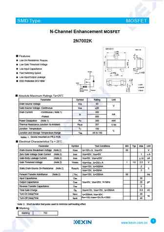
2n7002k.pdf
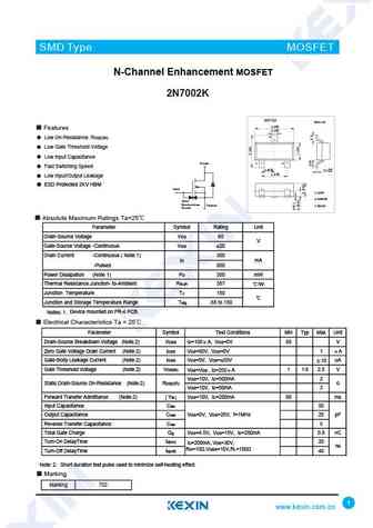
SMD Type MOSFET N-Channel Enhancement MOSFET 2N7002K SOT-23 Unit mm +0.1 2.9 -0.1 Features +0.1 0.4 -0.1 3 Low On-Resistance RDS(ON) Low Gate Threshold Voltage Low Input Capacitance D rai n 1 2 Fast Switching Speed +0.1 +0.05 0.95 -0.1 0.1 -0.01 +0.1 1.9 -0.1 Low Input/Output Leakage ESD Protected 2KV HBM Gate 1.Base 1 GATE 2.Emitter 2 SOURCE Gate Protectio... See More ⇒
2n7002k-3.pdf
SMD Type MOSFET N-Channel Enhancement MOSFET 2N7002K SOT-23-3 Unit mm +0.2 2.9-0.1 +0.1 0.4 -0.1 Features 3 Low On-Resistance RDS(ON) Low Gate Threshold Voltage Low Input Capacitance 1 2 D rai n +0.02 +0.1 0.15 -0.02 0.95 -0.1 Fast Switching Speed +0.1 1.9-0.2 Low Input/Output Leakage ESD Protected 2KV HBM Gate 1.Base 1 GATE 2.Emitter 2 SOURCE Gate Protect... See More ⇒
2n7002e-3.pdf
SMD Type MOSFET N-Channel Enhancement MOSFET 2N7002E SOT-23-3 Unit mm +0.2 2.9 -0.1 +0.1 0.4-0.1 3 Features Low On-Resistance RDS(ON) Low Gate Threshold Voltage 1 2 +0.02 Low Input Capacitance +0.1 0.15 -0.02 0.95 -0.1 +0.1 1.9 -0.2 Fast Switching Speed Low Input/Output Leakage 1.Base 1 GATE 2.Emitter 2 SOURCE 3 DRAIN Absolute Maximum Ratings Ta=25 Parameter Symbol... See More ⇒
2n7002-3.pdf

SMD Type MOSFET N-Channel Enhancement MOSFET 2N7002 SOT-23-3 Unit mm +0.2 2.9 -0.1 +0.1 0.4 -0.1 Features 3 High density cell design for low RDS(ON) Voltage controlled small signal switch Rugged and reliable 1 2 High saturation current capability +0.02 +0.1 0.15 -0.02 0.95-0.1 +0.1 1.9-0.2 1.Base 1 GATE 2.Emitter 2 SOURCE 3.collector 3 DRAIN Absolute Maximum Ratings... See More ⇒
2n7002t.pdf
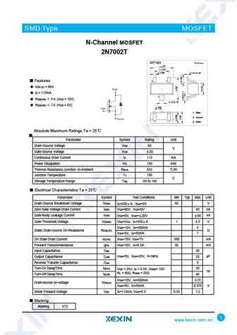
SMD Type MOSFET N-Channel MOSFET 2N7002T SOT-523 U nit m m +0. 1 1.6 -0. 1 +0.1 1.0 -0.1 +0.05 0.2 -0.05 0.15 0.05 2 1 Features VDS (V) = 60V ID = 115mA 3 RDS(ON) 5 (VGS = 10V) 0.3 0.05 RDS(ON) 7 (VGS = 5V) +0.1 0.5-0.1 1. Gate 2. Source 3. Drain Absolute Maximum Ratings Ta = 25 Parameter Symbol Rating Unit Drain-Source... See More ⇒
2n7002.pdf
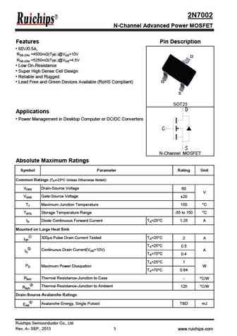
2N7002 N-Channel Advanced Power MOSFET Features Pin Description 60V/0.5A, RDS (ON) =4500m (Typ.)@VGS=10V D RDS (ON) =5250m (Typ.)@VGS=4.5V Low On-Resistance Super High Dense Cell Design Reliable and Rugged G Lead Free and Green Devices Available (RoHS Compliant) S SOT23 D Applications Power Management in Desktop Computer or DC/DC Converters G S N-C... See More ⇒
2n7002dw.pdf
2N7002DW 60V N-Channel Enhancement Mode MOSFET FEATURES RDS(ON), VGS@10V,IDS@500mA=5 RDS(ON), VGS@4.5V,IDS@75mA=7.5 Advanced Trench Process Technology High Density Cell Design For Ultra Low On-Resistance Specially Designed for Battery Operated Systems, Solid-State Relays Drivers Relays, Displays, Lamps, Solenoids, Memories, etc. In compliance with EU Ro... See More ⇒
2n7002.pdf
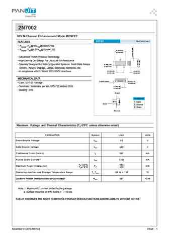
2N7002 60V N-Channel Enhancement Mode MOSFET FEATURES RDS(ON), VGS@10V,IDS@500mA=5 RDS(ON), VGS@4.5V,IDS@75mA=7.5 0.120(3.04) 0.110(2.80) Advanced Trench Process Technology High Density Cell Design For Ultra Low On-Resistance Specially Designed for Battery Operated Systems, Solid-State Relays 0.056(1.40) 0.047(1.20) Drivers Relays, Displays, Lamps, Solenoid... See More ⇒
2n7002kw.pdf
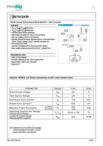
2N7002KW 60V N-Channel Enhancement Mode MOSFET - ESD Protected FEATURES RDS(ON), VGS@10V,IDS@500mA=3 RDS(ON), VGS@4.5V,IDS@200mA=4 Advanced Trench Process Technology High Density Cell Design For Ultra Low On-Resistance Very Low Leakage Current In Off Condition Specially Designed for Battery Operated Systems, Solid-State Relays Drivers Relays, Displays, La... See More ⇒
2n7002w.pdf
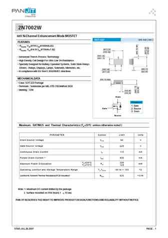
2N7002W 60V N-Channel Enhancement Mode MOSFET FEATURES RDS(ON), VGS@10V,IDS@500mA=5 RDS(ON), VGS@4.5V,IDS@75mA=7.5 Advanced Trench Process Technology High Density Cell Design For Ultra Low On-Resistance Specially Designed for Battery Operated Systems, Solid-State Relays Drivers Relays, Displays, Lamps, Solenoids, Memories, etc. In compliance with EU RoH... See More ⇒
2n7002k.pdf
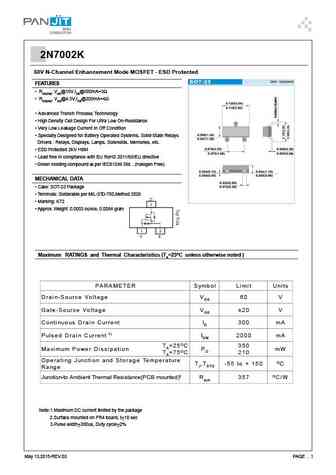
2N7002K 60V N-Channel Enhancement Mode MOSFET - ESD Protected FEATURES RDS(ON), VGS@10V,IDS@500mA=3 RDS(ON), VGS@4.5V,IDS@200mA=4 0.120(3.04) 0.110(2.80) Advanced Trench Process Technology High Density Cell Design For Ultra Low On-Resistance Very Low Leakage Current In Off Condition 0.056(1.40) Specially Designed for Battery Operated Systems, Solid-State R... See More ⇒
2n7002tb.pdf
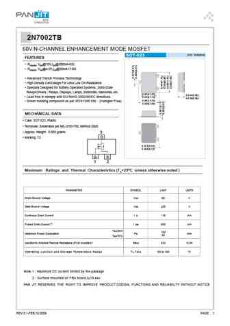
2N7002TB 60V N-CHANNEL ENHANCEMENT MODE MOSFET Unit inch(mm) SOT-523 FEATURES RDS(ON), VGS@10V,IDS@500mA=5 RDS(ON), VGS@4.5V,IDS@50mA=7.5 Advanced Trench Process Technology High Density Cell Design For Ultra Low On-Resistance Specially Designed for Battery Operated Systems, Solid-State Relays Drivers Relays, Displays, Lamps, Solenoids, Memories, etc. 0.... See More ⇒
2n7002kdw.pdf
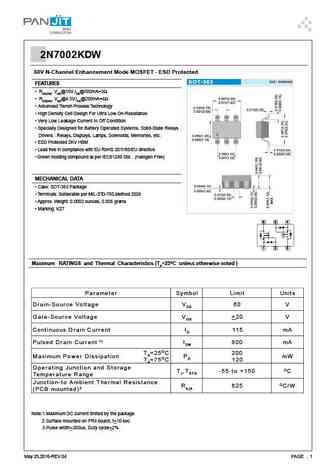
2N7002KDW 60V N-Channel Enhancement Mode MOSFET - ESD Protected FEATURES RDS(ON), VGS@10V,IDS@500mA=3 RDS(ON), VGS@4.5V,IDS@200mA=4 Advanced Trench Process Technology High Density Cell Design For Ultra Low On-Resistance Very Low Leakage Current In Off Condition Specially Designed for Battery Operated Systems, Solid-State Relays Drivers Relays, Displays, L... See More ⇒
2n7002ktb.pdf
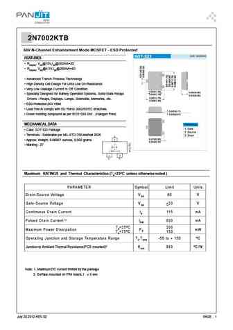
2N7002KTB 60V N-Channel Enhancement Mode MOSFET - ESD Protected FEATURES RDS(ON), VGS@10V,IDS@500mA=3 RDS(ON), VGS@4.5V,IDS@200mA=4 Advanced Trench Process Technology High Density Cell Design For Ultra Low On-Resistance Very Low Leakage Current In Off Condition 0.052(1.30) 0.024(0.60) Specially Designed for Battery Operated Systems, Solid-State Relays 0.... See More ⇒
am2n7002.pdf
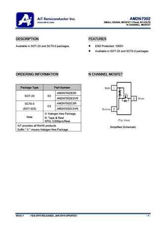
AiT Semiconductor Inc. AM2N7002 www.ait-ic.com SMALL SIGNAL MOSFET 115mA, 60 VOLTS N-CHANNEL MOSFET DESCRIPTION FEATURES Available in SOT-23 and SC70-3 packages. ESD Protected 1000V Available in SOT-23 and SC70-3 packages ORDERING INFORMATION N CHANNEL MOSFET Package Type Part Number AM2N7002E3R SOT-23 E3 AM2N7002E3VR SC70-3 AM2N7002C3R C3 (SOT-323) AM2N7002C3... See More ⇒
am2n7002k.pdf
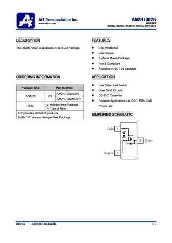
AiT Semiconductor Inc. AM2N7002K www.ait-ic.com MOSFET SMALL SIGNAL MOSFET 380mA, 60 VOLTS DESCRIPTION FEATURES The AM2N7002K is available in SOT-23 Package ESD Protected Low R DS(ON) Surface Mount Package RoHS Compliant Available in SOT-23 package ORDERING INFORMATION APPLICATION Low Side Load Switch Package Type Part Number Level Shift Circ... See More ⇒
am2n7002dw.pdf
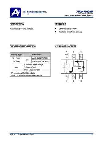
AiT Semiconductor Inc. AM2N7002DW www.ait-ic.com N-CHANNEL MOSFET SMALL SIGNAL MOSFET 115mA, 60 VOLTS DESCRIPTION FEATURES Available in SOT-363 package. ESD Protected 1000V Available in SOT-363 package ORDERING INFORMATION N CHANNEL MOSFET Package Type Part Number SOT-363 AM2N7002DWC6R C6 (SC70-6) AM2N7002DWC6VR V Halogen free Package Note R Tape & Reel SPQ ... See More ⇒
ama2n7002.pdf
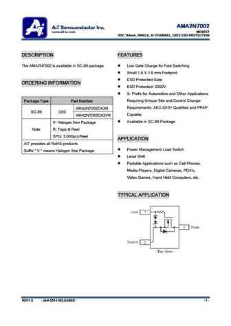
AMA2N7002 AiT Semiconductor Inc. www.ait-ic.com MOSFET 30V, 154mA, SINGLE, N-CHANNEL, GATE ESD PROTECTION DESCRIPTION FEATURES The AMA2N7002 is available in SC-89 package. Low Gate Charge for Fast Switching Small 1.6 X 1.6 mm Footprint ESD Protected Gate ORDERING INFORMATION ESD Protected 2000V S- Prefix for Automotive and Other Applications Requirin... See More ⇒
am2n7002w.pdf
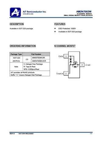
AiT Semiconductor Inc. AM2N7002W www.ait-ic.com N-CHANNEL MOSFET SMALL SIGNAL MOSFET 115mA, 60 VOLTS DESCRIPTION FEATURES Available in SOT-323 package. ESD Protected 1000V Available in SOT-323 package ORDERING INFORMATION N CHANNEL MOSFET Package Type Part Number SOT-323 AM2N702WC3R C3 (SC70-3) AM2N702WC3VR V Halogen free Package Note R Tape & Reel SPQ 3,0... See More ⇒
cmt2n7002 cmt2n7002wg.pdf
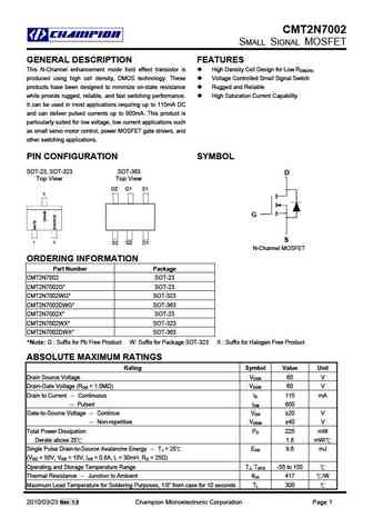
CMT2N7002 SMALL SIGNAL MOSFET GENERAL DESCRIPTION FEATURES This N-Channel enhancement mode field effect transistor is High Density Cell Design for Low RDS(ON) produced using high cell density, DMOS technology. These Voltage Controlled Small Signal Switch products have been designed to minimize on-state resistance Rugged and Reliable while provide rugged, reliable, and fast swi... See More ⇒
cmt2n7002k.pdf
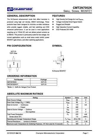
CMT2N7002K SMALL SIGNAL MOSFET GENERAL DESCRIPTION FEATURES This N-Channel enhancement mode field effect transistor is High Density Cell Design for Low RDS(ON) produced using high cell density, DMOS technology. These Voltage Controlled Small Signal Switch products have been designed to minimize on-state resistance Rugged and Reliable while provide rugged, reliable, and fast sw... See More ⇒
cmt2n7002ag.pdf
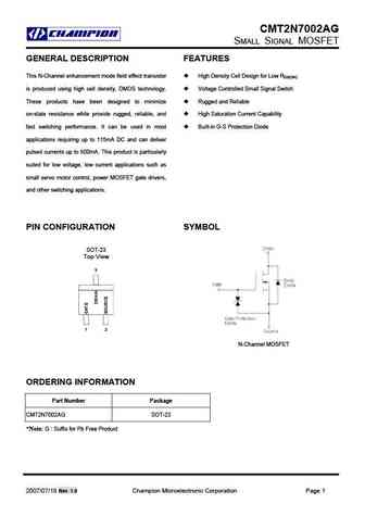
CMT2N7002AG SMALL SIGNAL MOSFET GENERAL DESCRIPTION FEATURES This N-Channel enhancement mode field effect transistor High Density Cell Design for Low RDS(ON) is produced using high cell density, DMOS technology. Voltage Controlled Small Signal Switch These products have been designed to minimize Rugged and Reliable on-state resistance while provide rugged, reliable, and High... See More ⇒
2n7002esgp.pdf
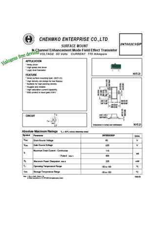
CHENMKO ENTERPRISE CO.,LTD 2N7002ESGP SURFACE MOUNT N-Channel Enhancement Mode Field Effect Transistor VOLTAGE 60 Volts CURRENT 115 mAmpere APPLICATION * Relay driver * High speed line driver * Logic level transistor SOT-23 FEATURE * Small surface mounting type. (SOT-23) * High density cell design for low RDS(ON). * Suitable for high packing density. * Rugged and reliable. (1)... See More ⇒
2n7002ssgp.pdf
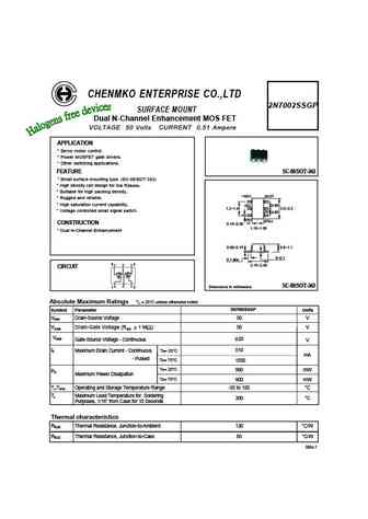
CHENMKO ENTERPRISE CO.,LTD 2N7002SSGP SURFACE MOUNT Dual N-Channel Enhancement MOS FET VOLTAGE 50 Volts CURRENT 0.51 Ampere APPLICATION * Servo motor control. * Power MOSFET gate drivers. * Other switching applications. FEATURE SC-88/SOT-363 * Small surface mounting type. (SC-88/SOT-363) * High density cell design for low RDS(ON). * Suitable for high packing density. (1) (G1) ... See More ⇒
2n7002sesgp.pdf
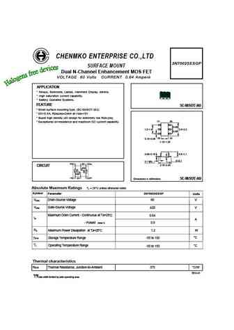
CHENMKO ENTERPRISE CO.,LTD 2N7002SESGP SURFACE MOUNT Dual N-Channel Enhancement MOS FET VOLTAGE 60 Volts CURRENT 0.64 Ampere APPLICATION * Relays, Solenoids, Lamps, Hammers Display deivers. * High saturation current capability. * Battery Operated Systems. FEATURE SC-88/SOT-363 * Small surface mounting type. (SC-88/SOT-363) . * 60V/0.5A, RDS(ON)=2ohm at VGS=10V * Super high d... See More ⇒
2n7002sgp.pdf
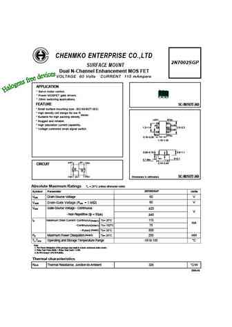
CHENMKO ENTERPRISE CO.,LTD 2N7002SGP SURFACE MOUNT Dual N-Channel Enhancement MOS FET VOLTAGE 60 Volts CURRENT 115 mAmpere APPLICATION * Servo motor control. * Power MOSFET gate drivers. * Other switching applications. FEATURE SC-88/SOT-363 * Small surface mounting type. (SC-88/SOT-363) * High density cell design for low R DS(ON). * Suitable for high packing density. (1) (S1)... See More ⇒
2n7002gp.pdf
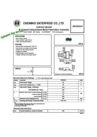
CHENMKO ENTERPRISE CO.,LTD 2N7002GP SURFACE MOUNT N-Channel Enhancement Mode Field Effect Transistor VOLTAGE 60 Volts CURRENT 115 mAmpere APPLICATION * Servo motor control. * Power MOSFET gate drivers. * Other switching applications. SOT-23 FEATURE * Small surface mounting type. (SOT-23) * High density cell design for low RDS(ON). * Suitable for high packing density. * Rugged ... See More ⇒
2n7002tesgp.pdf
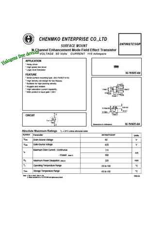
CHENMKO ENTERPRISE CO.,LTD 2N7002TESGP SURFACE MOUNT N-Channel Enhancement Mode Field Effect Transistor VOLTAGE 60 Volts CURRENT 115 mAmpere APPLICATION * Relay driver * High speed line driver * Logic level transistor SC-75/SOT-416 FEATURE * Small surface mounting type. (SC-75/SOT-416) * High density cell design for low RDS(ON). * Suitable for high packing density. 0.1 0.2 0.... See More ⇒
2n7002dsgp.pdf
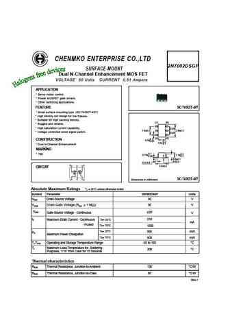
CHENMKO ENTERPRISE CO.,LTD 2N7002DSGP SURFACE MOUNT Dual N-Channel Enhancement MOS FET VOLTAGE 50 Volts CURRENT 0.51 Ampere APPLICATION * Servo motor control. * Power MOSFET gate drivers. * Other switching applications. FEATURE SC-74/SOT-457 * Small surface mounting type. (SC-74/SOT-457) * High density cell design for low RDS(ON). * Suitable for high packing density. (1) (6) *... See More ⇒
2n7002gp-a.pdf

CHENMKO ENTERPRISE CO.,LTD 2N7002GP-A SURFACE MOUNT N-Channel Enhancement Mode Field Effect Transistor VOLTAGE 60 Volts CURRENT 115 mAmpere APPLICATION * Servo motor control. * Power MOSFET gate drivers. * Other switching applications. SOT-23 FEATURE * Small surface mounting type. (SOT-23) * High density cell design for low RDS(ON). * Suitable for high packing density. * Rugge... See More ⇒
2n7002egp.pdf
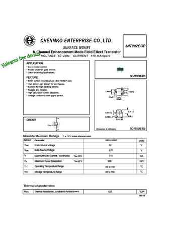
CHENMKO ENTERPRISE CO.,LTD 2N7002EGP SURFACE MOUNT N-Channel Enhancement Mode Field Effect Transistor VOLTAGE 60 Volts CURRENT 115 mAmpere APPLICATION * Servo motor control. * Power MOSFET gate drivers. * Other switching applications. SC-70/SOT-323 FEATURE * Small surface mounting type. (SC-70/SOT-323) * High density cell design for low RDS(ON). * Suitable for high packing dens... See More ⇒
2n7002esegp.pdf
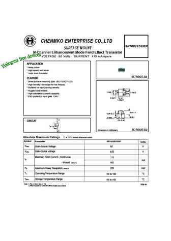
CHENMKO ENTERPRISE CO.,LTD 2N7002ESEGP SURFACE MOUNT N-Channel Enhancement Mode Field Effect Transistor VOLTAGE 60 Volts CURRENT 115 mAmpere APPLICATION * Relay driver * High speed line driver * Logic level transistor SC-70/SOT-323 FEATURE * Small surface mounting type. (SC-70/SOT-323) * High density cell design for low RDS(ON). * Suitable for high packing density. * Rugged and... See More ⇒
2n7002tgp.pdf
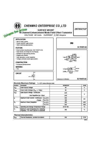
CHENMKO ENTERPRISE CO.,LTD 2N7002TGP SURFACE MOUNT N-Channel Enhancement Mode Field Effect Transistor VOLTAGE 60 Volts CURRENT 0.250 Ampere APPLICATION * Servo motor control. * Power MOSFET gate drivers. * Other switching applications. SC-75/SOT-416 FEATURE * Small surface mounting type. (SC-75/SOT-416) * High density cell design for low RDS(ON). * Suitable for high packing den... See More ⇒
2n7002vgp.pdf
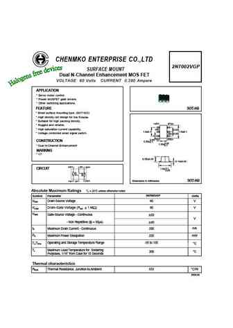
CHENMKO ENTERPRISE CO.,LTD 2N7002VGP SURFACE MOUNT Dual N-Channel Enhancement MOS FET VOLTAGE 60 Volts CURRENT 0.280 Ampere APPLICATION * Servo motor control. * Power MOSFET gate drivers. * Other switching applications. FEATURE SOT-563 * Small surface mounting type. (SOT-563) * High density cell design for low RDS(ON) * Suitable for high packing density. (1) (S1) (D1)(6) * Rug... See More ⇒
2n7002-g.pdf
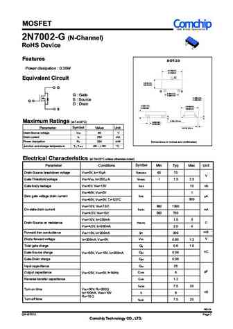
MOSFET 2N7002-G (N-Channel) RoHS Device Features SOT-23 Power dissipation 0.35W 0.119(3.00) 0.110(2.80) D Equivalent Circuit 0.056(1.40) 0.047(1.20) D G S 0.083(2.10) G Gate 0.066(1.70) 0.006(0.15) S Source 0.002(0.05) G D Drain 0.044(1.10) 0.103(2.60) 0.035(0.90) 0.086(2.20) S 0.006(0.15)max 0.020(0.50) Maximum Ratings (at TA=25 C) 0.013(0.35) Symbol 0.00... See More ⇒
ctm2n7002.pdf
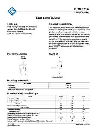
CTM2N7002 Crownpo Technology Small Signal MOSFET Features General Description High Density Cell Design for Low RDS(ON) This N-Channel enhancement mode field effect transistor Voltage Controlled Small Signal Switch is produced using high cell density,DMOS technology.These Rugged and Reliable products have been designed to minimize on-state High Saturation Current Capability resistance... See More ⇒
2n7002k.pdf
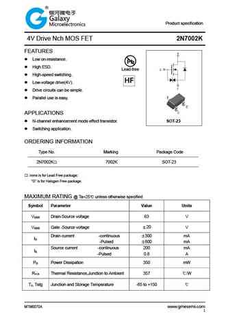
Product specification 4V Drive Nch MOS FET 2N7002K FEATURES Low on-resistance. Pb High ESD. Lead-free High-speed switching. Low-voltage drive(4V). Drive circuits can be simple. Parallel use is easy. APPLICATIONS N-channel enhancement mode effect transistor. SOT-23 Switching application. ORDERING INFORMATION Type No. Marking Packag... See More ⇒
2n7002h 2n7002hw 2n7002ht 2n7002hl.pdf
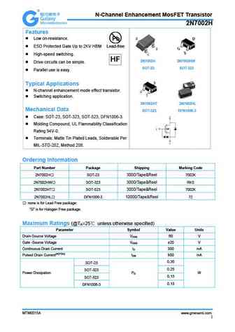
N-Ch Enhancem osFET Tra hannel E ment Mo ansistor 2N N7002H Feature es Low on-resistanc ce. Pb ESD Protected G 2KV HBM Lead-free Gate Up to 2 High- ching. -speed switc 2N7002H 2N7002H HW Drive n be simple. e circuits can SOT-23 SOT-323 T 2 Parallel use is ea asy. Typica ations al Applica N-channel enhan ode effect tra ncement mo ansistor. Switc ation... See More ⇒
2n7002k.pdf
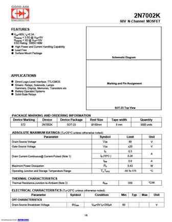
2N7002K 60V N-Channel MOSFET FEATURES VDS=60V, ID=0.3A RDS(ON) ... See More ⇒
k2n7002k.pdf
K2N7002K N-Channel Enhancement Mode MOSFET 2018.04.18 2018.04.18 2018.04.18 2018.04.18 1 000 2017.10.18 2 001 2018.04.18 3 1 of 7 AUK Dalian K2N7002K N-Channel Enh... See More ⇒
me2n7002d.pdf
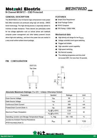
ME2N7002D N-Channel MOSFET ESD Protected GENERAL DESCRIPTION FEATURES Simple Drive Requirement The ME2N7002D is the N-Channel logic enhancement mode power Small Package Outline field effect transistors are produced using high cell density , DMOS ROHS Compliant trench technology. This high density process is especially tailored to ESD Rating = 2000V HBM min... See More ⇒
me2n7002e.pdf
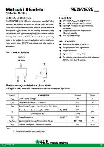
ME2N7002E N-Channel MOSFET GENERAL DESCRIPTION FEATURES 60V / 0.50A , RDS(ON)= 5.0 @VGS=10V The ME2N7002E is the N-Channel enhancement mode field effect 60V / 0.30A , RDS(ON)= 5.5 @VGS=4.5V transistors are produced using high cell density DMOS technology. Super high density cell design for extremely These products have been designed to minimize on-state resistanc... See More ⇒
2n7002k.pdf
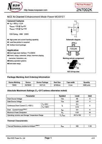
Pb Free Product http //www.ncepower.com 2N7002K NCE N-Channel Enhancement Mode Power MOSFET General Features VDS = 60V,ID = 0.3A RDS(ON) ... See More ⇒
a2n7002k.pdf
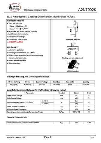
http //www.ncepower.com A2N7002K NCE Automotive N-Channel Enhancement Mode Power MOSFET General Features V = 60V,I = 0.3A DS D R ... See More ⇒
pz2n7002m.pdf
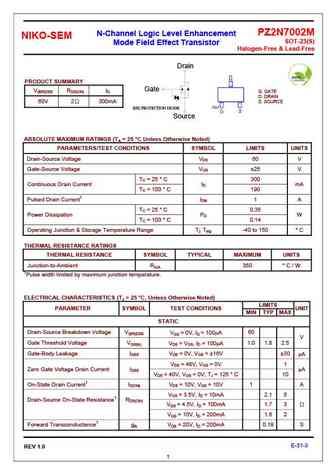
PZ2N7002M N-Channel Logic Level Enhancement NIKO-SEM SOT-23(S) Mode Field Effect Transistor Halogen-Free & Lead-Free Drain PRODUCT SUMMARY Gate V(BR)DSS RDS(ON) ID G. GATE D. DRAIN 60V 2 300mA S. SOURCE ESD PROTECTION DIODE Source ABSOLUTE MAXIMUM RATINGS (TA = 25 C Unless Otherwise Noted) PARAMETERS/TEST CONDITIONS SYMBOL LIMITS UNITS Drain-Source Voltage VDS... See More ⇒
2n7002.pdf
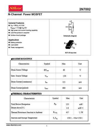
2N7002 N-Channel Power MOSFET D General Features VDS = 60V,ID =0.115A G RDS(ON) ... See More ⇒
2n7002kw.pdf
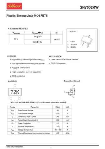
2N7002KW Plastic-Encapsulate MOSFETS N-Channel MOSFET SOT-323 I V(BR)DSS RDS(on)MAX D 3 5K@10V 60 V 340mA 1. GATE 5.3K@4.5V 2. SOURCE 1 2 3. DRAIN FEATURE APPLICATION Load Switch for Portable Devices z Highdensity celldesign for Low R DS(on) DC/DC Converter z Voltagecontrolled smallsignal switch z Rugged andreliable z High saturation current capability z ESD pro... See More ⇒
2n7002e.pdf
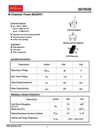
2N7002E N-Channel Power MOSFET General Features VDS = 60V,ID = 300mA RDS(ON) ... See More ⇒
2n7002k.pdf
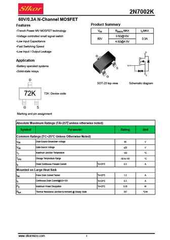
2N7002K 60V/0.3A N-Channel MOSFET Product Summary Features Trench Power MV MOSFET technology VDS RDS(ON) MAX ID MAX Voltage controlled small signal switch 3.5 @10VD2 60V S1 0.3A D1 Low input Capacitance 4.5 @4.5V Fast Switching Speed Low Input / Output Leakage D Application Battery operated systems S Solid-state relays G D SOT-23 top view Schematic dia... See More ⇒
2n7002kdw.pdf
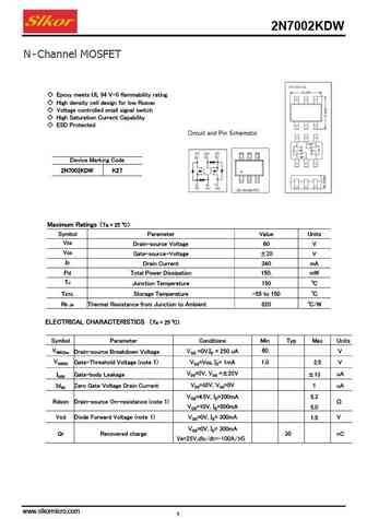
2N7002KDW N- Channel MOSFET Epoxy meets UL 94 V-0 flammability rating High density cell design for low RDS(ON) Voltage controlled small signal switch High Saturation Current Capability ESD Protected Device Marking Code 2N7002KDW K27 Maximum Ratings Ta = 25 Symbol Parameter Value Units VDS Drain-source Voltage 60 V VGS Gate-source-Voltage 20 V ... See More ⇒
2n7002kt.pdf
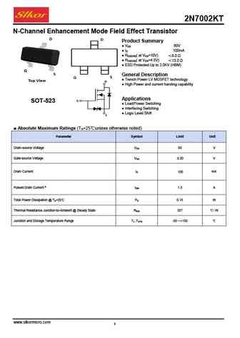
2N7002KT N-Channel Enhancement Mode Field Effect Transistor Product Summary V 60V DS I 100mA D R ( at V =10V) 8.0 DS(ON) GS R ( at V =4.5V) 13.0 DS(ON) GS ESD Protected Up to 2.0KV (HBM) General Description Trench Power LV MOSFET technology High Power and current handing capability Applications SOT-523 Load/Power Switching Int... See More ⇒
2n7002wsk.pdf
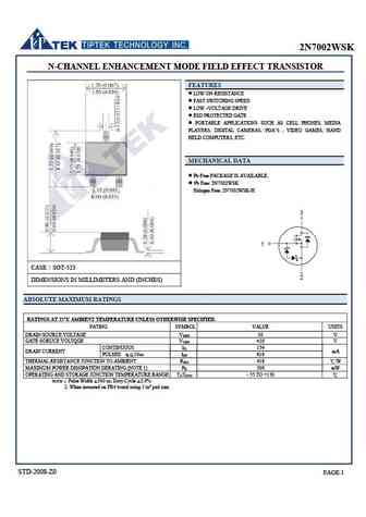
2N7002WSK N-CHANNEL ENHANCEMENT MODE FIELD EFFECT TRANSISTOR FEATURES LOW ON-RESISTANCE FAST SWITCHING SPEED LOW VOLTAGE DRIVE ESD PROTECTED GATE PORTABLE APPLICATIONS SUCH AS CELL PHONES, MEDIA PLAYERS, DIGITAL CAMERAS, PDA S , VIDEO GAMES, HAND HELD COMPUTERS, ETC. MECHANICAL DATA Pb-Free PACKAGE IS AVAILABLE. Pb Free 2N7002WSK H... See More ⇒
s2n7002dm.pdf
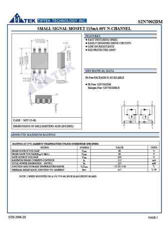
S2N7002DM SMALL SIGNAL MOSFET 115mA 60V N-CHANNEL FEATURES FAST SWITCHING SPEED. EASILY DESIGNED DRIVE CIRCUITS. LOW ON-RESISTANCE ESD PROTECTED 1000V MECHANICAL DATA Pb-Free PACKAGE IS AVAILABLE. Pb Free S2N7002DM Halogen Free S2N7002DM-H CASE SOT-23-6L DIMENSIONS IN MILLIMETERS AND (INCHES) ABSOLUTE MAXIMUM RATINGS RATINGS AT 25 C AMBIEN... See More ⇒
qm2n7002e3k1.pdf
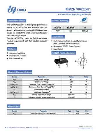
QM2N7002E3K1 N-Ch 60V Fast Switching MOSFETs General Description Product Summery The QM2N7002E3K1 is the highest performance trench N-CH MOSFETs with extreme high cell BVDSS RDSON ID density , which provide excellent RDSON and gate 60V 3 180mA charge for most of the small power switching and load switch applications. Applications The QM2N7002E3K1 meet the RoHS and Green ... See More ⇒
2n7002b.pdf
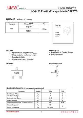
R UMW UMW 2N7002B UMW 2N7002B UMW 2N7002B UMW 2N7002B UMW 2N7002B UMW 2N7002B - SOT 23 Plastic-Encapsulate MOSFETS 2N7002B MOSFET (N-Channel) ID V(BR)DSS RDS(on)MAX SOT-23 5 @10V 60V 115mA 7 @5V 1. GATE 2. SOURCE 3. DRAIN APPLICATION FEATURE Load Switch for Portable Devices High density cell design for low RDS(ON) DC/DC Converter Voltage co... See More ⇒
2n7002ta 2n7002tc.pdf
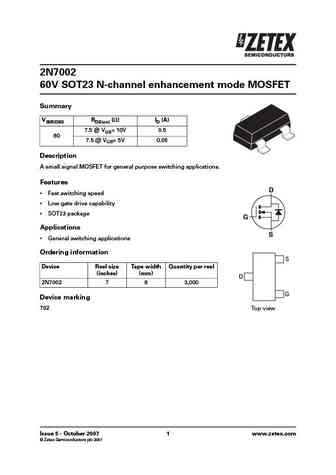
2N7002 60V SOT23 N-channel enhancement mode MOSFET Summary V(BR)DSS RDS(on) ( )ID (A) 7.5 @ VGS= 10V 0.5 60 7.5 @ VGS= 5V 0.05 Description A small signal MOSFET for general purpose switching applications. Features D Fast switching speed Low gate drive capability SOT23 package G Applications S General switching applications Ordering information S Device Reel ... See More ⇒
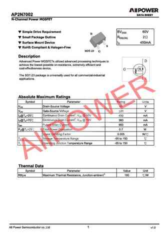
2n7002ew.pdf
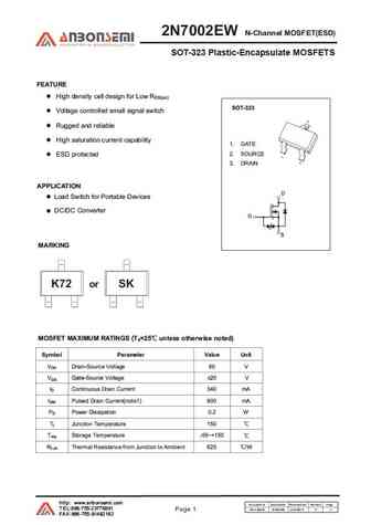
2N7002EW N-Channel MOSFET(ESD) SOT-323 Plastic-Encapsulate MOSFETS FEATURE High density cell design for Low RDS(on) SOT-323 Voltage controlled small signal switch Rugged and reliable High saturation current capability 1. GATE 2. SOURCE ESD protected 3. DRAIN APPLICATION ... See More ⇒
2n7002e.pdf
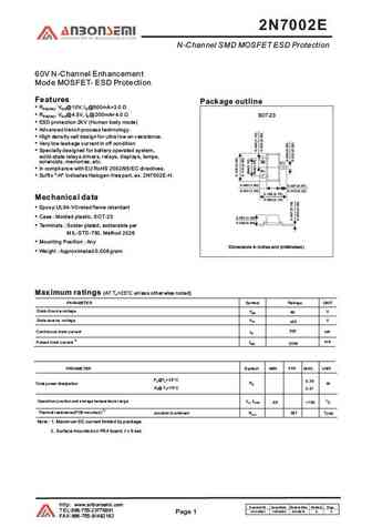
2N7002E N-Channel SMD MOSFET ESD Protection 60V N-Channel Enhancement Mode MOSFET- ESD Protection Features Package outline RDS(ON), VGS@10V, ID@500mA=3.0 RDS(ON), VGS@4.5V, ID@200mA=4.0 SOT-23 ESD protection 2 V (Human body mode) Advanced trench process technology. High density cell design for ultra low on-resistance. Very low leakage current in off c... See More ⇒
2n7002t.pdf
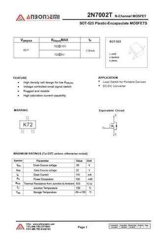
2N7002T N-Channel MOSFET SOT-523 Plastic-Encapsulate MOSFETS ID V(BR)DSS RDS(on)MAX SOT-523 1. GATE 2. SOURCE 3. DRAIN APPLICATION FEATURE High density cell design for low RDS(ON) Voltage controlled ... See More ⇒
2n7002et.pdf
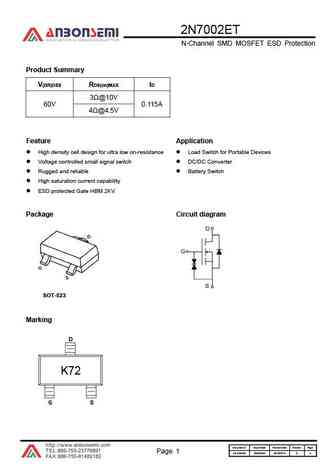
2N7002ET N-Channel SMD MOSFET ESD Protection Product Summary V R I (BR)DSS DS(on)MAX D 3 @10V 60V 0.115A 4 @4.5V Feature Application High density cell design for ultra low on-resistance Load Switch for Portable Devices Voltage controlled small signal switch DC/DC Converter Rugged and reliable Battery Switch High saturation current capability ... See More ⇒
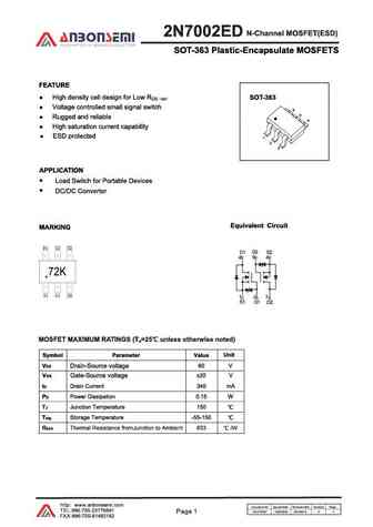
2n7002.pdf
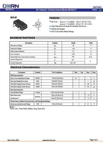
2N7002 MOSFET ROHS N-Channel Enhancement-Mode MOSFET SOT-23 - Features 60V/0.2A, RDS(ON) = 7.5 (MAX) @VGS = 10V. Id = 0.5A RDS(ON) = 7.5 (MAX) @VGS = 5V . Id = 0.05A Super High dense cell design for extremely low RDS(ON) . Reliable and Rugged. SOT-23 for Surface Mount Package. MAXIMUM RANTINGS Parameter Symbol Limit Units Drain-Source Voltage VDS 60 V Gat... See More ⇒
2n7002k.pdf
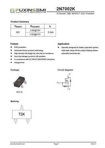
2N7002K N-Channel SMD MOSFET ESD Protection Product Summary V(BR)DSS RDS(on)MAX ID 2.8 @10V 60V 0.34A 3.6 @4.5V Feature Application ESD protection Specially designed for battery operated system, Advanced trench process technology solid-state relays drivers,relays,displays,lamps, High density cell design for ultra low on-resistance solenoids,memories,etc. Very low leaka... See More ⇒
2n7002kd.pdf
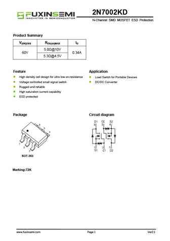
2N7002KD N-Channel SMD MOSFET ESD Protection Product Summary V(BR)DSS RDS(on)MAX ID 5.0 @10V 60V 0.34A 5.3 @4.5V Feature Application High density cell design for ultra low on-resistance Load Switch for Portable Devices Voltage controlled small signal switch DC/DC Converter Rugged and reliable High saturation current capability ESD protected Package Circuit diagram... See More ⇒
et2n7002k.pdf
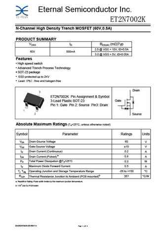
Eternal Semiconductor Inc. ET2N7002K N-Channel High Density Trench MOSFET (60V,0.5A) PRODUCT SUMMARY VDSS ID RDS(on) (m )Typ 2.5 @ VGS = 10V, ID=0.5A 60V 500mA 3.0 @ VGS = 5V, ID=0.05A Features High speed switch Advanced Trench Process Technology SOT-23 package ESD protected up to 2KV Lead Pb -free and halogen-free Drain ET2N7002K Pin Assignment & Symbo... See More ⇒
2n7002.pdf
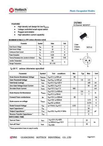
Plastic-Encapsulate Mosfets 2N7002 FEATURE N-Channel MOSFET High density cell design for low RDS(ON) Voltage controlled small signal switch Rugged and reliable High saturation current capability MAXIMUM RATINGS (Ta=25 unless otherwise noted) Parameter Symbol Value Unit 1.Gate Drain-Source Voltage VDS 60 V 2.Source SOT-23 3.Drain Gate-Source Voltage VGS 20 V Cont... See More ⇒
2n7002k.pdf
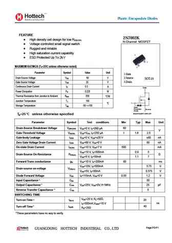
Plastic-Encapsulate Diodes FEATURE 2N7002K High density cell design for low RDS(ON) N-Channel MOSFET Voltage controlled small signal switch Rugged and reliable High saturation current capability ESD Protected Up To 2k V MAXIMUM RATINGS (Ta=25 unless otherwise noted) Parameter Symbol Value Unit 1.Gate Drain-Source Voltage VDS 60 V 2.Source SOT-23 3.Drain Gate-Sou... See More ⇒
hss2n7002k.pdf
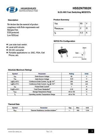
HSS2N7002K N-Ch 60V Fast Switching MOSFETs Product Summary Description VDS 60 V We declare that the material of product compliance with Rohs requirements and RDS(ON),max 2 Halogen Free. ESD protected ID 0.3 A Low RDS(on) SOT23 Pin Configuration l Low side load switch l Level shift circutis l DC-DC converter l Portable applications i.e. DSC, PDA, Cell Phone, ... See More ⇒
2n7002.pdf
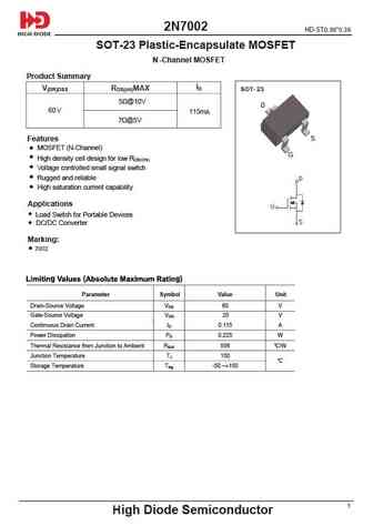
2N7002 HD-ST0.36*0.36 SOT-23 Plastic-Encapsulate MOSFET N -Channel MOSFET roduct Summary P ID V(BR)DSS RDS(on)MAX SOT- 23 5 @10V D 60V 115mA 7 @5V S Features MOSFET (N-Channel) G High density cell design for low RDS(ON) Voltage controlled small signal switch Rugged and reliable High saturation current capability Applications ... See More ⇒
2n7002k.pdf
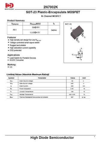
2N7002K SOT-23 Plastic-Encapsulate MOSFET N -Channel MOSFET roduct Summary P ID V(BR)DSS RDS(on)MAX SOT- 23 5 @10V D 60V mA 340 @4.5V 5.3 S Features High density cell design for Low RDS on G Voltage controlled small signal switch Rugged and reliable High saturation current capability ESD protected Applications Load ... See More ⇒
jmtd2n7002ks.pdf
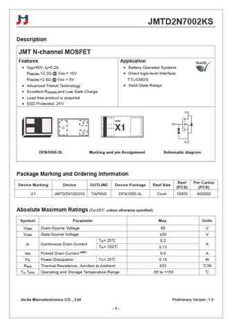
JMTD2N7002KS Description JMT N-channel MOSFET Features Application V =60V, I =0.2A Battery Operated Systems DS D R ... See More ⇒
jmtla2n7002ks.pdf
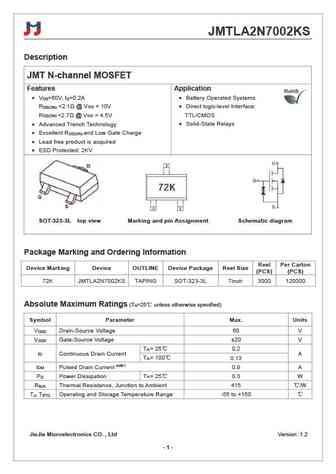
JMTLA2N7002KS Description JMT N-channel MOSFET Features Application V =60V, I =0.2A Battery Operated Systems DS D R ... See More ⇒
jmtl2n7002ks.pdf
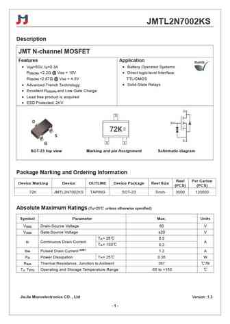
JMTL2N7002KS Description JMT N-channel MOSFET Features Application V =60V, I =0.3A Battery Operated Systems DS D R ... See More ⇒
jmtlb2n7002kds.pdf
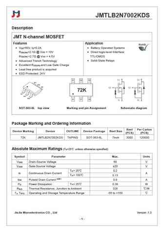
JMTLB2N7002KDS Description JMT N-channel MOSFET Features Application V =60V, I =0.2A Battery Operated Systems DS D R ... See More ⇒
2n7002.pdf
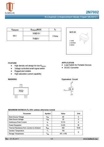
2N7002 N-Channel Enhancement Mode Power MOSFET ID V(BR)DSS RDS(on)MAX SOT-23 5 @10V 60V 115mA 7 @5V 1. GATE 2. SOURCE 3. DRAIN APPLICATION FEATURE Load Switch for Portable Devices High density cell design for low RDS(ON) DC/DC Converter Voltage controlled small signal switch Rugged and reliable High saturation current capability Equivale... See More ⇒
2n7002kt.pdf
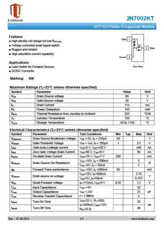
2N7002KT SOT-523 Plastic-Encapsulate Mosfets Features Gate 1 High density cell design for low R DS (ON) Voltage controlled small signal switch 3 Drain Rugged and reliable High saturation current capability Source 2 Applications (Top View) Load Switch for Portable Devices DC/DC Converter Marking KN Maximum Ratings (T =25 C unless otherwise spe... See More ⇒
2n7002k.pdf
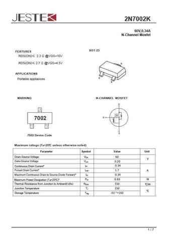
2N7002K 60V,0.34A N-Channel Mosfet SOT-23 FEATURES RDS(ON) 2.3 @VGS=10V RDS(ON) 2.7 @VGS=4.5V APPLICATIONS Portable appliances MARKING N-CHANNEL MOSFET 7002 Device Code Maximum ratings (Ta=25 unless otherwise noted) Parameter Symbol Value Unit Drain-Source Voltage VDS 60 V Gate-Source Voltage VGS 20 I 0.34 D* Continuous Drain Current* Pulsed Drain Current* ... See More ⇒
2n7002.pdf
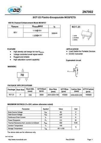
2N7002 SOT-23 Plastic-Encapsulate MOSFETS 60V N-Channel Enhancement Mode MOSFET V(BR)DSS RDS(on)MAX ID SO T -23 3 1.1 @10V 60V mA 500 @4.5V 1.3 1. GATE 2. SOURCE 1 2 3. DRAIN FEATURE APPLICATION Load Switch for Portable Devices High density cell design for low RDS(ON) DC/DC Converter Voltage controlled small signal switch Rugged and reliable Hig... See More ⇒
2n7002k.pdf
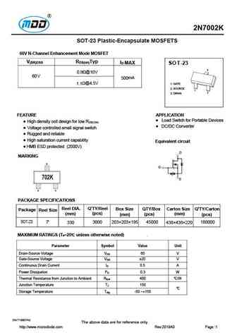
2N7002K SOT-23 Plastic-Encapsulate MOSFETS 60V N-Channel Enhancement Mode MOSFET V(BR)DSS RDS(on)Typ ID MAX SO T -23 3 0.9 @10V 60V mA 500 @4.5V 1.1 1. GATE 2. SOURCE 1 2 3. DRAIN FEATURE APPLICATION Load Switch for Portable Devices High density cell design for low RDS(ON) DC/DC Converter Voltage controlled small signal switch Rugged and reliable ... See More ⇒
2n7002kw.pdf
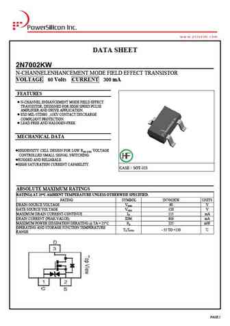
DATA SHEET 2N7002KW N-CHANNELENHANCEMENT MODE FIELD EFFECT TRANSISTOR VOLTAGE 60 Volts CURRENT 300 mA FEATURES N-CHANNEL ENHANCEMENT MODE FIELD EFFECT TRANSISTOR, DESIGNED FOR HIGH SPEED PULSE AMPLIFIER AND DRIVE APPLICATION. ESD MIL-STD883 , 1KV CONTACT DISCHARGE COMPLIANT PROTECTION. LEAD FREE AND HALOGEN-FREE. MECHANICAL DATA HIGDENSITY CELL DESIGN FOR LOW RDS... See More ⇒
2n7002.pdf
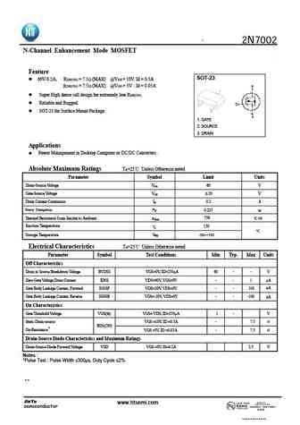
2N7002 N-Channel Enhancement Mode MOSFET Feature SOT-23 60V/0.2A, RDS(ON) = 7.5 (MAX) @VGS = 10V. Id = 0.5A RDS(ON) = 7.5 (MAX) @VGS = 5V . Id = 0.05A Super High dense cell design for extremely low RDS(ON) . Reliable and Rugged. SOT-23 for Surface Mount Package. 1. GATE 2. SOURCE 3. DRAIN Applications Power Management in Desktop Computer or DC/DC Converters ... See More ⇒
2n7002k.pdf
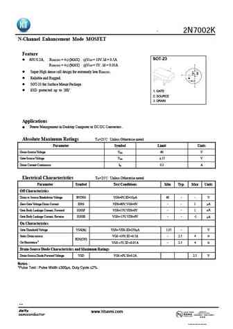
2N7002K N-Channel Enhancement Mode MOSFET Feature SOT-23 60V/0.2A, RDS(ON) = 4 (MAX) @VGS = 10V. Id = 0.5A RDS(ON) = 4 (MAX) @VGS = 5V . Id = 0.05A Super High dense cell design for extremely low RDS(ON) . Reliable and Rugged. SOT-23 for Surface Mount Package. ESD protected up to 2K V 1. GATE 2. SOURCE 3. DRAIN Applications Power Management in Desktop Comp... See More ⇒
agm2n7002.pdf
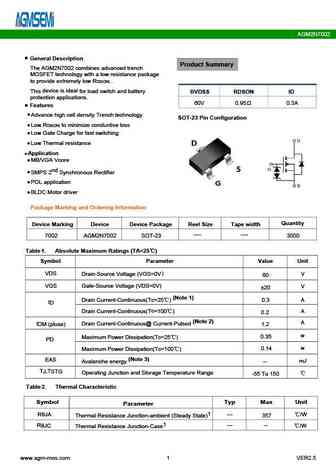
AGM2N7002 General Description Product Summary The AGM2N7002 combines advanced trench MOSFET technology with a low resistance package to provide extremely low R . DS(ON) device is ideal This for load switch and battery BVDSS RDSON ID protection applications. 60V 0.95 0.3A Features Advance high cell density Trench technology SOT-23 Pin Configuration Low R to mi... See More ⇒
agm2n7002k3.pdf
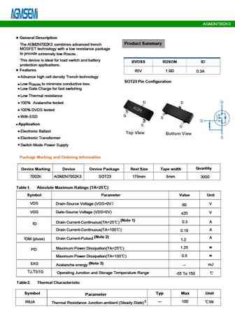
AGM2N7002K3 Typical Performance Characteristics www.agm-mos.com 3 VER2.65 AGM2N7002K3 SOT23 Marking Instructions www.agm-mos.com 5 VER2.65 AGM2N7002K3 Disclaimer The information provided in this document is believed to be accurate and reliable. However,Shenzhen Core Control Source Electronics Technology Co., Ltd. does not assume any responsibility for the following consequence... See More ⇒
2n7002.pdf
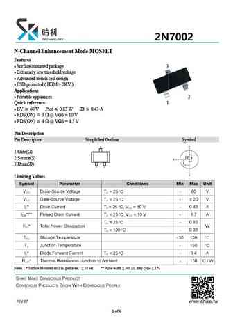
N-Channel Enhancement Mode MOSFET Channel Enhancement Mode MOSFET Features Surface-mounted package 3 Extremely low threshold voltage Advanced trench cell design ESD protected ( HBM > 2KV ) Applications Portable appliances 2 Quick reference 1 1 BV 60 V Ptot 0.83 W ID 0.43 A BV 60 V Ptot 0.83 W ID 0.43 A RDS(ON) 3 @ VGS =... See More ⇒
2n7002t.pdf
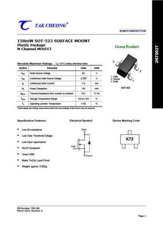
TAK CHEONG SEMICONDUCTOR 150mW SOT-523 SURFACE MOUNT Plastic Package Green Product N-Channel MOSFET 3 Absolute Maximum Ratings TA = 25 C unless otherwise noted Symbol Parameter Value Units 2 VDS Drain-Source Voltage 60 V 1. Gate VGS Continuous Gate-Source Voltage 20V V 2. Source 1 3. Drain ID Continuous Drain Current 115 mA SOT-523 PD Power Dissipation 1... See More ⇒
2n7002k.pdf
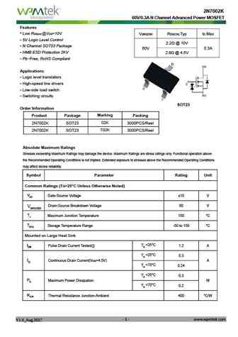
2N7002K 60V/0.3A N Channel Advanced Power MOSFET Features Low RDS(on) @VGS=10V V R Typ I Max (BR)DSS DS(ON) D 5V Logic Level Control 2.2 @ 10V N Channel SOT23 Package 60V 0.3A HMB ESD Protection 2KV 2.8 @ 4.5V Pb-Free, RoHS Compliant Applications Logic level translators High-speed line drivers Low-side load switch Switching circu... See More ⇒
2n7002kw.pdf
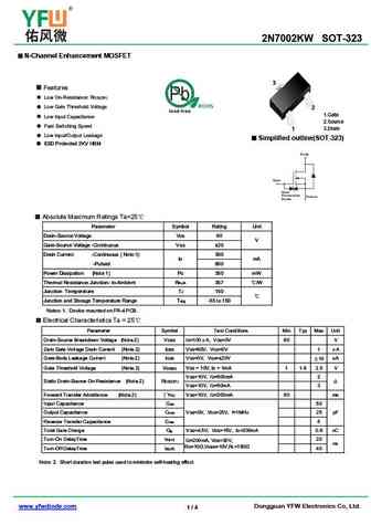
2N7002KW SOT-323 N-Channel Enhancement MOSFET 3 Features Low On-Resistance RDS(ON) Low Gate Threshold Voltage 2 1.Gate Low Input Capacitance 2.Source Fast Switching Speed 3.Drain 1 Low Input/Output Leakage Simplified outline(SOT-323) ESD Protected 2KV HBM Drai n Gate Gate Protection Source Diode Absolute Maximum Ratings Ta=25 Parameter Symbol Rating Unit Drain... See More ⇒
2n7002ak.pdf
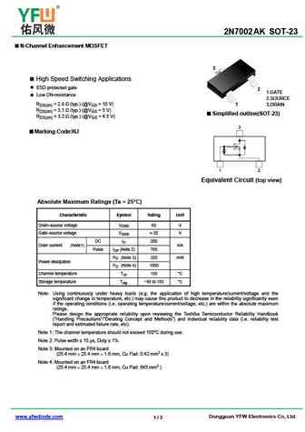
A 2N7002 K SOT-23 N-Channel Enhancement MOSFET 3 High Speed Switching Applications ESD protected gate 2 1.GATE Low ON-resistance 2.SOURCE RDS(on) = 2.8 (typ.) (@VGS = 10 V) 3.DRAIN 1 RDS(on) = 3.1 (typ.) (@VGS = 5 V) Simplified outline(SOT-23) RDS(on) = 3.2 (typ.) (@VGS = 4.5 V) 3 Marking Code NJ 1 2 Equivalent Circuit (top view) Absolute Maximum Ratings ... See More ⇒
2n7002k.pdf
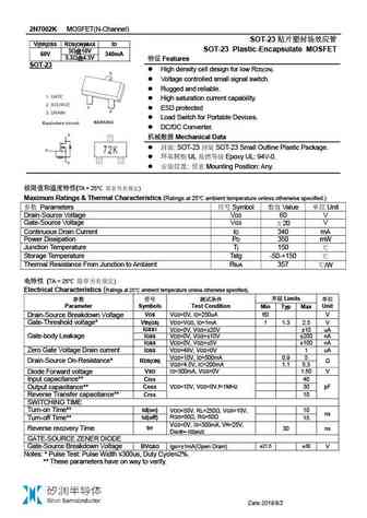
2N7002K MOSFET(N-Channel) SOT-23 V(BR)DSS RDS(ON)MAX ID SOT-23 Plastic-Encapsulate MOSFET 5 @10V 60V 340mA 5.3 @4.5V Features SOT-23 High density cell design for low RDS(ON). Voltage controlled small signal switch. Rugged and reliable. High saturation current capability. ESD protected Load Switch for Portable... See More ⇒
2n7002k.pdf

SHENZHEN LONG JING MICRO-ELECTRONICS CO., LTD. SOT-23 Plastic-Encapsulate Mosfets 2N7002K N-Channel Mosfet Features High density cell design for low R DS (ON) Voltage controlled small signal switch Rugged and reliable High saturation current capability ESD protected up to 2KV 1. Gate Marking 702 2. Source 3. Drain Maximum Ratings (T =25 C unless otherwise... See More ⇒
2n7002.pdf
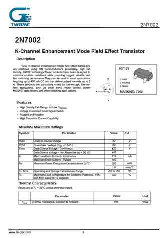
MMBT5551 2N7002 AO3400 SI2305 2N7002 N-Channel Enhancement Mode Field Effect Transistor Description These N-channel enhancement mode field effect transis-tors SOT-23 are produced using ON Semiconductor's proprietary, high cell density, DMOS technology.These products have been designed to minimize on-state resistance while providing rugged, reliable, and fast switching performan... See More ⇒
wst2n7002.pdf
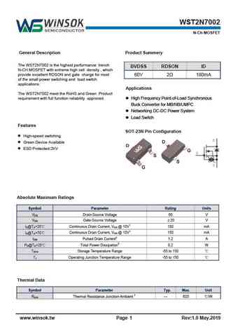
WST2N7002 N-Ch MOSFET General Description Product Summery The WST2N7002 is the highest performance trench BVDSS RDSON ID N-CH MOSFET with extreme high cell density , which provide excellent RDSON and gate charge for most 60V 2 180mA of the small power switching and load switch applications. Applications The WST2N7002 meet the RoHS and Green Product requirement with full ... See More ⇒
wst2n7002a.pdf
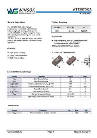
WST2N7002A N-Ch MOSFET General Description Product Summery The WST2N7002A is the highest BVDSS RDSON ID performance trench N-Ch MOSFET with extreme high cell density , which provide 60V 0.14 700mA excellent RDSON and gate charge for most of the small power switching and load switch Applications applications. The WST2N7002A meet the RoHS and Green Product requirement wi... See More ⇒
wst2n7002k.pdf
WST2N7002K N-Ch MOSFET Product Summery General Description The WST2N7002K is the highest performance BVDSS RDSON ID trench N-Ch MOSFET with extreme high cell density , which provide excellent RDSON and 60V 1 300mA gate charge for most of the small power switching and load switch applications. Applications The WST2N7002K meet the RoHS and Green Product requirement with... See More ⇒
se2n7002k.pdf
SHANGHAI July 2008 MICROELECTRONICS CO., LTD. SE2N7002K 60V,300mA N-Channel MOSFET Revision A General Description Features The MOSFETs from SINO-IC provide VDS (V) = 60V the best combination of fast switching, low ID = 300mA on-resistance and cost-effectiveness. RDS(ON) ... See More ⇒
se2n7002.pdf
SHANGHAI July 2008 MICROELECTRONICS CO., LTD. SE2N7002 60V,300mA N-Channel MOSFET Revision A General Description Features The MOSFETs from SINO-IC provide VDS (V) = 60V the best combination of fast switching, low ID = 300mA on-resistance and cost-effectiveness. RDS(ON) ... See More ⇒
vs2n7002k.pdf
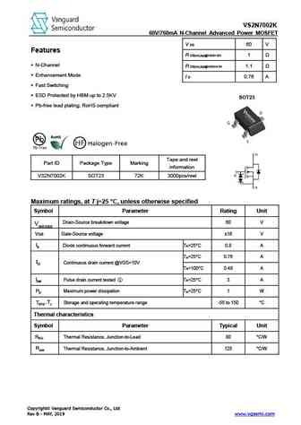
VS2N7002K 60V/760mA N-Channel Advanced Power MOSFET V DS 60 V Features R DS(on),typ@VGS=10V 1 N-Channel R DS(on),typ@VGS=4.5V 1.1 Enhancement Mode I D 0.76 A Fast Switching ESD Protected by HBM up to 2.5KV SOT23 Pb-free lead plating; RoHS compliant Tape and reel Part ID Package Type Marking information VS2N7002K SOT23 72K 3000pcs/reel... See More ⇒
2n7002e.pdf

2N7002E www.VBsemi.tw N-Channel 60-V (D-S) MOSFET FEATURES PRODUCT SUMMARY Halogen-free According to IEC 61249-2-21 VDS (V) RDS(on) ( )ID (mA) Definition 2.8 at VGS = 10 V 60 250 Low Threshold 2 V (typ.) Low Input Capacitance 25 pF Fast Switching Speed 25 ns Low Input and Output Leakage SOT-23 TrenchFET Power MOSFET 1200V ESD Protection G 1 ... See More ⇒
2n7002kb.pdf
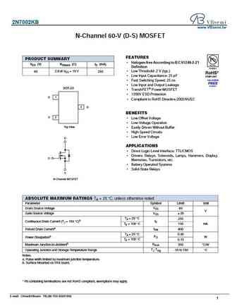
2N7002KB www.VBsemi.tw N-Channel 60-V (D-S) MOSFET FEATURES PRODUCT SUMMARY Halogen-free According to IEC 61249-2-21 VDS (V) RDS(on) ( )ID (mA) Definition 2.8 at VGS = 10 V 60 250 Low Threshold 2 V (typ.) Low Input Capacitance 25 pF Fast Switching Speed 25 ns Low Input and Output Leakage SOT-23 TrenchFET Power MOSFET 1200V ESD Protection G 1 ... See More ⇒
2n7002t.pdf

2N7002T www.VBsemi.tw N-Channel 60-V (D-S) MOSFET FEATURES PRODUCT SUMMARY Halogen-free According to IEC 61249-2-21 VDS (V) RDS(on) ( )ID (mA) Definition 2.8 at VGS = 10 V 60 250 Low Threshold 2 V (typ.) Low Input Capacitance 25 pF Fast Switching Speed 25 ns Low Input and Output Leakage SOT-23 TrenchFET Power MOSFET 1200V ESD Protection G 1 ... See More ⇒
2n7002bk.pdf
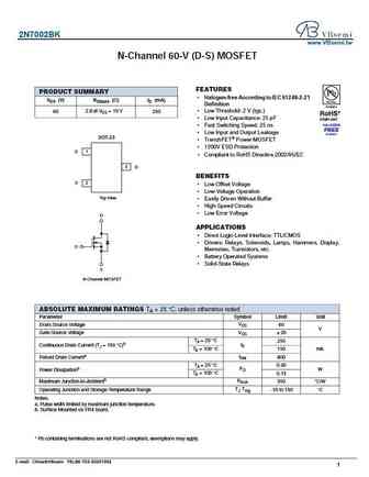
2N7002BK www.VBsemi.tw N-Channel 60-V (D-S) MOSFET FEATURES PRODUCT SUMMARY Halogen-free According to IEC 61249-2-21 VDS (V) RDS(on) ( )ID (mA) Definition 2.8 at VGS = 10 V 60 250 Low Threshold 2 V (typ.) Low Input Capacitance 25 pF Fast Switching Speed 25 ns Low Input and Output Leakage SOT-23 TrenchFET Power MOSFET 1200V ESD Protection G 1 ... See More ⇒

2n7002em3t5g.pdf
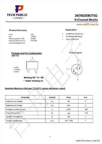
Marking RK * Or RK * =wafer tracking no ... See More ⇒
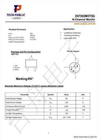
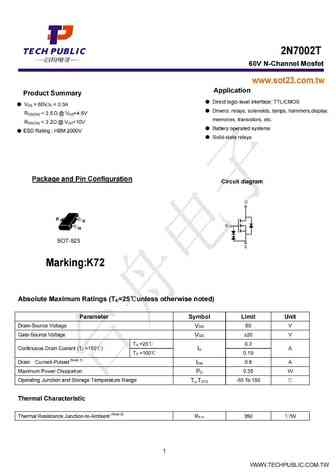
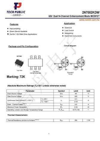
2n7002dw.pdf
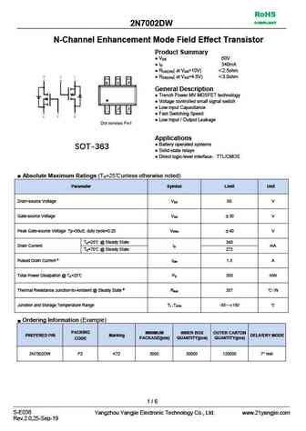
RoHS COMPLIANT 2N7002DW N-Channel Enhancement Mode Field Effect Transistor Product Summary V 60V DS I 340mA D R ( at V =10V) 2.5ohm DS(ON) GS R ( at V =4.5V) 3.0ohm DS(ON) GS General Description Trench Power MV MOSFET technology Voltage controlled small signal switch Low input Capacitance Fast Switching Speed Low Input /... See More ⇒
2n7002.pdf
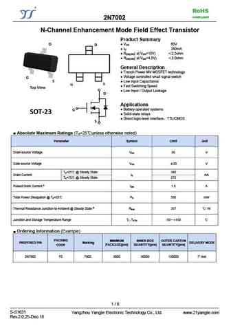
RoHS COMPLIANT 2N7002 N-Channel Enhancement Mode Field Effect Transistor Product Summary V 60V DS I 340mA D R ( at V =10V) 2.5ohm DS(ON) GS R ( at V =4.5V) 3.0ohm DS(ON) GS General Description Trench Power MV MOSFET technology Voltage controlled small signal switch Low input Capacitance Fast Switching Speed Low Input / O... See More ⇒
2n7002k.pdf
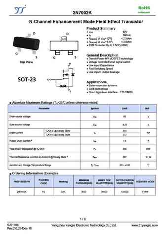
RoHS COMPLIANT 2N7002K N-Channel Enhancement Mode Field Effect Transistor Product Summary V 60V DS I 340mA D R ( at V =10V) 2.5ohm DS(ON) GS R ( at V =4.5V) 3.0ohm DS(ON) GS ESD Protected Up to 2.5KV (HBM) General Description Trench Power MV MOSFET technology Voltage controlled small signal switch Low input Capacitance F... See More ⇒
2n7002kdw.pdf
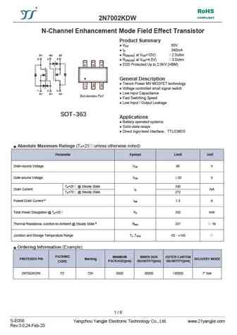
RoHS COMPLIANT 2N7002KDW N-Channel Enhancement Mode Field Effect Transistor Product Summary V 60V DS I 340mA D R ( at V =10V) 2.5ohm DS(ON) GS R ( at V =4.5V) 3.0ohm DS(ON) GS ESD Protected Up to 2.5KV (HBM) General Description Trench Power MV MOSFET technology Voltage controlled small signal switch Low input Capacitance ... See More ⇒
ttx2n7002ka.pdf
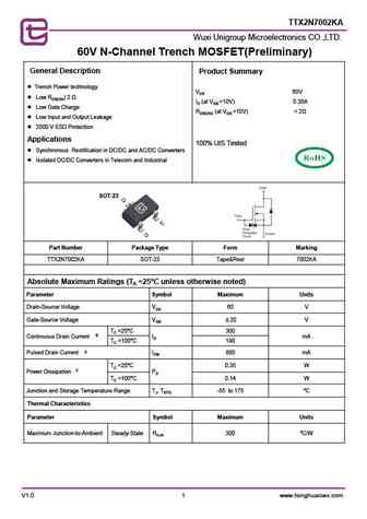
TTX2N7002KA Wuxi Unigroup Microelectronics CO.,LTD. 60V N-Channel Trench MOSFET(Preliminary) General Description Product Summary Trench Power technology VDS 60V Low RDS(ON) 2 ID (at VGS =10V) 0.35A Low Gate Charge RDS(ON) (at VGS =10V) ... See More ⇒
2n7000.pdf
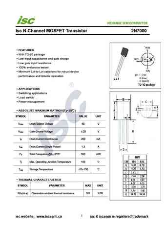
INCHANGE Semiconductor Isc N-Channel MOSFET Transistor 2N7000 FEATURES With TO-92 package Low input capacitance and gate charge Low gate input resistance 100% avalanche tested Minimum Lot-to-Lot variations for robust device performance and reliable operation APPLICATIONS Switching applications Load switch Power management ABSOLUTE MAXIMUM RATINGS(T =25 ) a ... See More ⇒
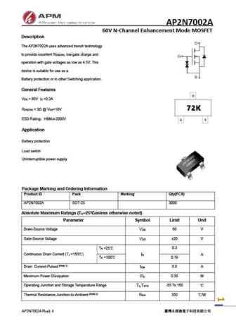
Detailed specifications: 2N6969JANTX , 2N6969JANTXV , 2N7000 , 2N7000P , 2N7001 , 2N7002 , 2N7002L , 2N7004 , AO3400 , 2N7006 , 2N7007 , 2N7008 , 2N7012 , 2N7013 , 2N7014 , 2N7016 , 2N7022 .
Keywords - 2N7005 MOSFET specs
2N7005 cross reference
2N7005 equivalent finder
2N7005 pdf lookup
2N7005 substitution
2N7005 replacement
Learn how to find the right MOSFET substitute. A guide to cross-reference, check specs and replace MOSFETs in your circuits.
🌐 : EN ES РУ

LIST
Last Update
MOSFET: AON5802 | AOSS62934 | AOSN21319C | AONS66966 | AONR62992 | AON7400B | AON6578 | AO3480C | AO3400C | HAF1008S
Popular searches
2n3053 transistor | 2sc458 replacement | bc557 transistor | 2n3638 | tip127 datasheet | irlz24n | irf620 | irfp350