FDMS3660AS Specs and Replacement
Type Designator: FDMS3660AS
Type of Transistor: MOSFET
Type of Control Channel: N-Channel
Absolute Maximum Ratings
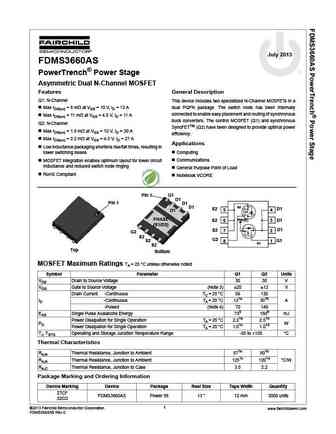
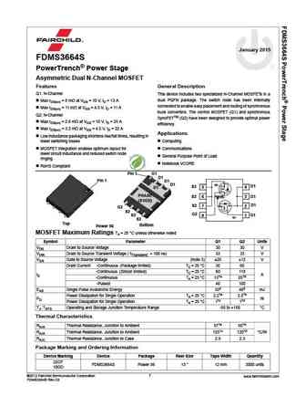
Pd ⓘ - Maximum Power Dissipation: 2.2 W
|Vds|ⓘ - Maximum Drain-Source Voltage: 30 V
|Vgs|ⓘ - Maximum Gate-Source Voltage: 20 V
|Id| ⓘ - Maximum Drain Current: 13 A
Tj ⓘ - Maximum Junction Temperature: 150 °C
Electrical Characteristics
tr ⓘ - Rise Time: 3 nS
Cossⓘ - Output Capacitance: 397 pF
RDSonⓘ - Maximum Drain-Source On-State Resistance: 0.008 Ohm
Package: PQFN5X6
FDMS3660AS substitution
- MOSFET ⓘ Cross-Reference Search
FDMS3660AS datasheet
fdms3660as.pdf
July 2013 FDMS3660AS PowerTrench Power Stage Asymmetric Dual N-Channel MOSFET Features General Description Q1 N-Channel This device includes two specialized N-Channel MOSFETs in a dual PQFN package. The switch node has been internally Max rDS(on) = 8 m at VGS = 10 V, ID = 13 A connected to enable easy placement and routing of synchronous Max rDS(on) = 11 m at VGS = 4.5 V, ... See More ⇒
fdms3660s.pdf
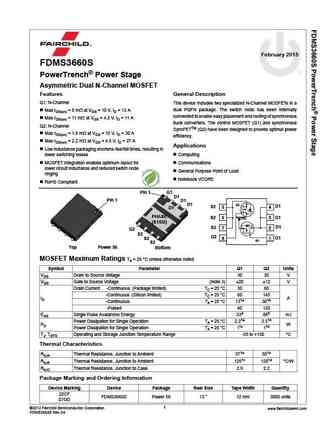
February 2015 FDMS3660S PowerTrench Power Stage Asymmetric Dual N-Channel MOSFET Features General Description Q1 N-Channel This device includes two specialized N-Channel MOSFETs in a dual PQFN package. The switch node has been internally Max rDS(on) = 8 m at VGS = 10 V, ID = 13 A connected to enable easy placement and routing of synchronous Max rDS(on) = 11 m at VGS = 4.5 ... See More ⇒
fdms3660s.pdf
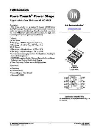
FDMS3660S PowerTrench) Power Stage Asymmetric Dual N-Channel MOSFET Description This device includes two specialized N-Channel MOSFETs in a www.onsemi.com dual PQFN package. The switch node has been internally connected to enable easy placement and routing of synchronous buck converters. The control MOSFET (Q1) and synchronous SyncFET (Q2) have been designed to provide optimal power ef... See More ⇒
fdms3668s.pdf
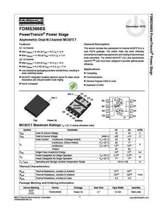
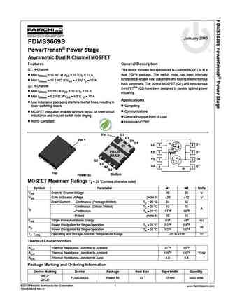
December 2012 FDMS3668S PowerTrench Power Stage Asymmetric Dual N-Channel MOSFET Features General Description Q1 N-Channel This device includes two specialized N-Channel MOSFETs in a dual PQFN package. The switch node has been internally Max rDS(on) = 8 m at VGS = 10 V, ID = 13 A connected to enable easy placement and routing of synchronous Max rDS(on) = 11 m at VGS = 4.5 ... See More ⇒
Detailed specifications: FDMS86350 , FDU6N25 , HUF76419SF085 , FDMS86252L , FDMS86550 , FDMA908PZ , FDS6679 , FCD620N60ZF , RFP50N06 , FDMS86202 , FQPF2N80YDTU , FCP190N60GF102 , FDB42AN15F085 , FDPF7N50U , FQP2N40 , FCP104N60F , FCH47N60FF085 .
History: DMP3085LSD
Keywords - FDMS3660AS MOSFET specs
FDMS3660AS cross reference
FDMS3660AS equivalent finder
FDMS3660AS pdf lookup
FDMS3660AS substitution
FDMS3660AS replacement
Need a MOSFET replacement? Our guide shows you how to find a perfect substitute by comparing key parameters and specs
History: DMP3085LSD
🌐 : EN ES РУ
LIST
Last Update
MOSFET: ASB80R750E | ASB70R380E | ASB65R300E | ASB65R220E | ASB65R120EFD | ASB60R150E | ASA80R900E | ASA80R750E | ASA80R290E | ASA70R950E
Popular searches
2sa640 | 2sb527 | 30g124 | 75339p mosfet | a968 transistor | f1010e mosfet | 2sc3883 | c3306 datasheet
