SSF2N60F Specs and Replacement
Type Designator: SSF2N60F
Type of Transistor: MOSFET
Type of Control Channel: N -Channel
Absolute Maximum Ratings
Pd ⓘ - Maximum Power Dissipation: 23 W
|Vds|ⓘ - Maximum Drain-Source Voltage: 600 V
|Vgs|ⓘ - Maximum Gate-Source Voltage: 30 V
|Id| ⓘ - Maximum Drain Current: 2 A
Tj ⓘ - Maximum Junction Temperature: 150 °C
Electrical Characteristics
tr ⓘ - Rise Time: 7.4 nS
Cossⓘ - Output Capacitance: 40 pF
Rds ⓘ - Maximum Drain-Source On-State Resistance: 4 Ohm
Package: TO220F
SSF2N60F substitution
SSF2N60F datasheet
ssf2n60f.pdf
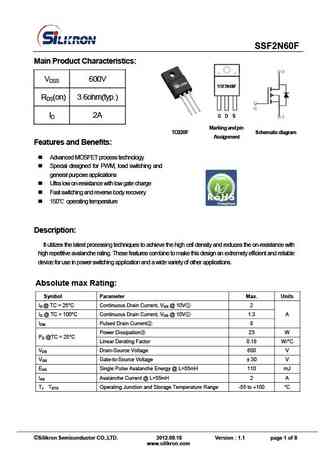
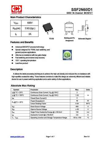
SSF2N60F Main Product Characteristics VDSS 600V RDS(on) 3.6ohm(typ.) ID 2A Marking a nd p in Sche ma ti c di agr a m TO220F Assignment Features and Benefits Advanced MOSFET process technology Special designed for PWM, load switching and general purpose applications Ultra low on-resistance with low gate charge Fast switching and reverse body recove... See More ⇒
ssf2n60.pdf
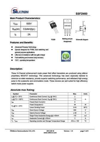
SSF2N60 Main Product Characteristics VDSS 600V RDS(on) 3.6ohm(typ.) ID 2A TO220 Marking and pin Schematic diagram Assignment Features and Benefits Advanced Process Technology Special designed for PWM, load switching and general purpose applications Ultra low on-resistance with low gate charge Fast switching and reverse body recovery 150 operating temper... See More ⇒
ssf2n60d.pdf
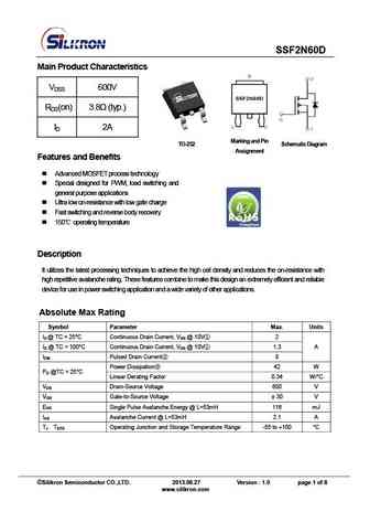
SSF2N60D Main Product Characteristics VDSS 600V RDS(on) 3.8 (typ.) ID 2A Marking and P in S che ma ti c Diag r am TO-252 Assignment Features and Benefits Advanced MOSFET process technology Special designed for PWM, load switching and general purpose applications Ultra low on-resistance with low gate charge Fast switching and reverse body recovery ... See More ⇒
ssf2n60g.pdf

SSF2N60G Main Product Characteristics VDSS 600V RDS(on) 3.5 (typ.) ID 2A TO-251 Marking and p in S che ma ti c di ag ra m Assignment Features and Benefits Advanced MOSFET process technology Special designed for PWM, load switching and general purpose applications Ultra low on-resistance with low gate charge Fast switching and reverse body recovery ... See More ⇒
Detailed specifications: SSF2814E , SSF2814EH2 , SSF2816E , SSF2816EB , SSF2841 , SSF2N60 , SSF2N60D , SSF2N60D2 , IRFP250 , SSF2N60G , SSF3002EG1 , SSF3018 , SSF3018D , SSF3028C1 , SSF3036C , SSF3051G7 , SSF3055 .
Keywords - SSF2N60F MOSFET specs
SSF2N60F cross reference
SSF2N60F equivalent finder
SSF2N60F pdf lookup
SSF2N60F substitution
SSF2N60F replacement
Learn how to find the right MOSFET substitute. A guide to cross-reference, check specs and replace MOSFETs in your circuits.


LIST
Last Update
MOSFET: APG045N85 | APG042N01D | APG038N01G | APG035N04Q | APG032N04G | APG028N10 | APG024N04G | APG022N06G | APG020N01GD | APG013N04G
Popular searches
c3203 transistor | irfp450 equivalent | 2sb649 | 2sb324 transistor | b754 transistor | 2sc828 equivalent | 4843ns | 2sc1318 datasheet