SSF3056C Specs and Replacement
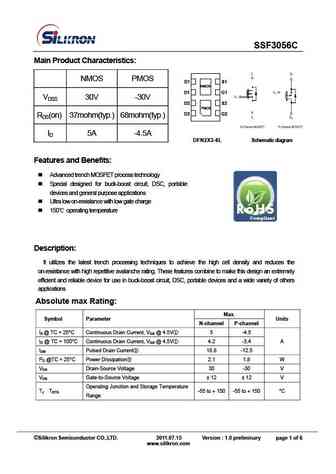
Type Designator: SSF3056C
Type of Transistor: MOSFET
Type of Control Channel: NP-Channel
Absolute Maximum Ratings
Pd ⓘ - Maximum Power Dissipation: 2.1 W
|Vds|ⓘ - Maximum Drain-Source Voltage: 30 V
|Vgs|ⓘ - Maximum Gate-Source Voltage: 12 V
|Id| ⓘ - Maximum Drain Current: 5(4.5) A
Tj ⓘ - Maximum Junction Temperature: 150 °C
Electrical Characteristics
RDSonⓘ - Maximum Drain-Source On-State Resistance: 0.055(0.085) Ohm
Package: DFN2X3-8L
SSF3056C substitution
- MOSFET ⓘ Cross-Reference Search
SSF3056C datasheet
ssf3056c.pdf
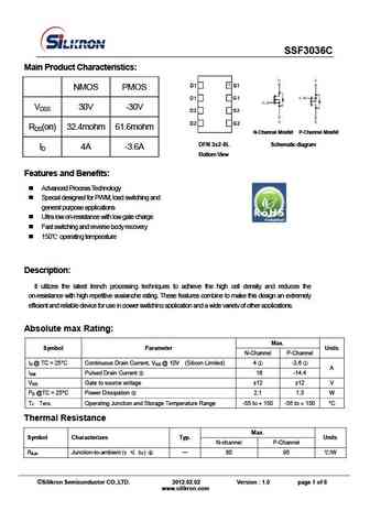
SSF3056C Main Product Characteristics NMOS PMOS D1 S1 D1 S1 NMOS NMOS D1 G1 D1 G1 VDSS 30V -30V D2 S2 D2 S2 PMOS PMOS D2 G2 D2 G2 RDS(on) 37mohm(typ.) 68mohm(typ.) ID 5A -4.5A DFN2X3-8L Schematic diagram Bottom View Features and Benefits Advanced trench MOSFET process technology Special designed for buck-boost circuit, DSC, portable devices and gene... See More ⇒
ssf3055.pdf
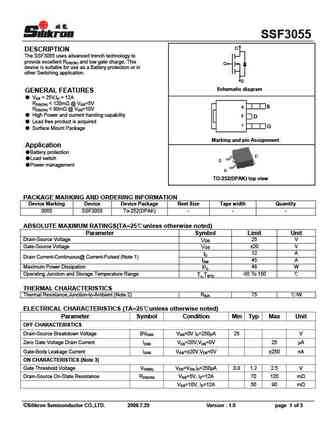
SSF3055 D DESCRIPTION The SSF3055 uses advanced trench technology to provide excellent RDS(ON) and low gate charge. This G device is suitable for use as a Battery protection or in other Switching application. S Schematic diagram GENERAL FEATURES VDS = 25V,ID = 12A RDS(ON) ... See More ⇒
ssf3051g7.pdf
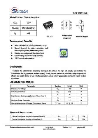
SSF3051G7 Main Product Characteristics D VDSS -30V G RDS(on) 45mohm(typ.) S ID -4A Marking and pin SOT23-6 Schematic diagram Assignment Features and Benefits Advanced trench MOSFET process technology Special designed for buttery protection, load switching and general power management Ultra low on-resistance with low gate charge Fast switching and rev... See More ⇒
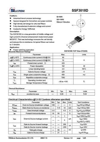
ssf3018.pdf
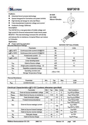
SSF3018 Feathers ID=60A Advanced trench process technology BV=100V Special designed for Convertors and power controls Rdson=15mohm High density cell design for ultra low Rdson Fully characterized Avalanche voltage and current Avalanche Energy 100% test Description The SSF3018 is a new generation of middle voltage and high current N Channel enhancement mode t... See More ⇒
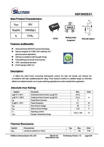
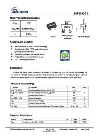
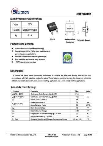
Detailed specifications: SSF2N60G, SSF3002EG1, SSF3018, SSF3018D, SSF3028C1, SSF3036C, SSF3051G7, SSF3055, 20N50, SSF3092G1, SSF3117, SSF32E0E, SSF3314E, SSF3322, SSF3324, SSF3338, SSF3339
Keywords - SSF3056C MOSFET specs
SSF3056C cross reference
SSF3056C equivalent finder
SSF3056C pdf lookup
SSF3056C substitution
SSF3056C replacement
Need a MOSFET replacement? Our guide shows you how to find a perfect substitute by comparing key parameters and specs
