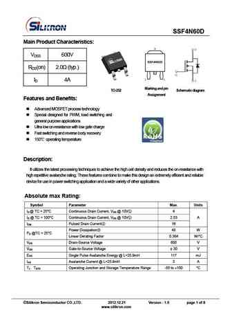
SSF4NS60D Specs and Replacement
Type Designator: SSF4NS60D
Type of Transistor: MOSFET
Type of Control Channel: N-Channel
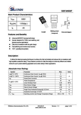
Absolute Maximum Ratings
Pd ⓘ - Maximum Power Dissipation: 50 W
|Vds|ⓘ - Maximum Drain-Source Voltage: 600 V
|Vgs|ⓘ - Maximum Gate-Source Voltage: 30 V
|Id| ⓘ - Maximum Drain Current: 4 A
Tj ⓘ - Maximum Junction Temperature: 150 °C
Electrical Characteristics
tr ⓘ - Rise Time: 17.6 nS
Cossⓘ - Output Capacitance: 222 pF
RDSonⓘ - Maximum Drain-Source On-State Resistance: 1.2 Ohm
Package: TO252
SSF4NS60D substitution
- MOSFET ⓘ Cross-Reference Search
SSF4NS60D datasheet
ssf4ns60d.pdf
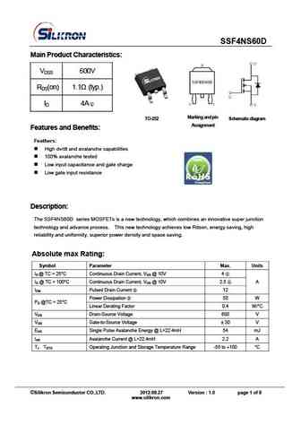
SSF4NS60D Main Product Characteristics VDSS 600V RDS(on) 1.1 (typ.) ID 4A TO-252 Marking a nd p in Sche ma ti c di agr a m Assignment Features and Benefits Feathers High dv/dt and avalanche capabilities 100% avalanche tested Low input capacitance and gate charge Low gate input resistance Description The SSF4NS60D series MOSFETs is a new te... See More ⇒
ssf4n90as.pdf
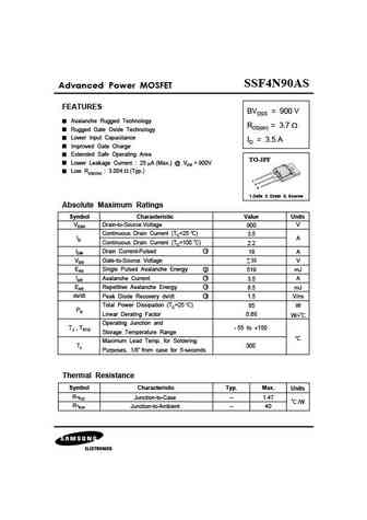
SSF4N90AS Advanced Power MOSFET FEATURES BVDSS = 900 V Avalanche Rugged Technology RDS(on) = 3.7 Rugged Gate Oxide Technology Lower Input Capacitance ID = 3.5 A Improved Gate Charge Extended Safe Operating Area TO-3PF Lower Leakage Current 25 A (Max.) @ VDS = 900V Low RDS(ON) 3.054 (Typ.) 1 2 3 1.Gate 2. Drain 3. Source Absolute Maximum Ratings Symbol Ch... See More ⇒
ssf4n80as.pdf
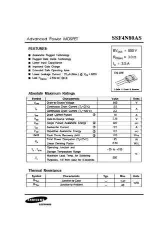
SSF4N80AS Advanced Power MOSFET FEATURES BVDSS = 800 V Avalanche Rugged Technology RDS(on) = 3.0 Rugged Gate Oxide Technology Lower Input Capacitance ID = 3.5 A Improved Gate Charge Extended Safe Operating Area TO-3PF Lower Leakage Current 25 A (Max.) @ VDS = 800V Low RDS(ON) 2.450 (Typ.)c 1 2 3 1.Gate 2. Drain 3. Source Absolute Maximum Ratings Symbol C... See More ⇒
ssf4n60g.pdf

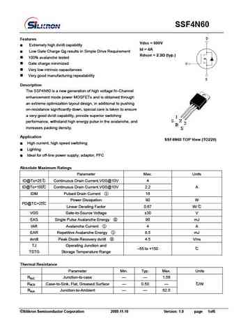
SSF4N60G Main Product Characteristics VDSS 600V RDS(on) 1.85 (typ.) ID 4A TO-251 Marking and p in S che ma ti c di ag ra m Assignment Features and Benefits Advanced MOSFET process technology Special designed for PWM, load switching and general purpose applications Ultra low on-resistance with low gate charge Fast switching and reverse body recovery ... See More ⇒
Detailed specifications: SSF4703, SSF4703DC, SSF47NS60H, SSF4953, SSF4N60, SSF4N60D, SSF4N60F, SSF4N60G, IRF630, SSF53A0E, SSF5506, SSF5508A, SSF5508U, SSF5N50D, SSF5N60D, SSF5N60F, SSF5N60G
Keywords - SSF4NS60D MOSFET specs
SSF4NS60D cross reference
SSF4NS60D equivalent finder
SSF4NS60D pdf lookup
SSF4NS60D substitution
SSF4NS60D replacement
Step-by-step guide to finding a MOSFET replacement. Cross-reference parts and ensure compatibility for your repair or project.
History: AP9998GI-HF
🌐 : EN ES РУ

LIST
Last Update
MOSFET: FTF30P35D | FTF25N35DHVT | FTF15N35D | FTE15C35G | FTP02P15G | FTE02P15G | AKF30N5P0SX | AKF30N10S | AKF20P45D | CM4407
Popular searches
30g124 | 75339p mosfet | a968 transistor | f1010e mosfet | 2sc3883 | c3306 datasheet | hy3810 | c711 transistor