SSPL2090 Specs and Replacement
Type Designator: SSPL2090
Type of Transistor: MOSFET
Type of Control Channel: N-Channel
Absolute Maximum Ratings
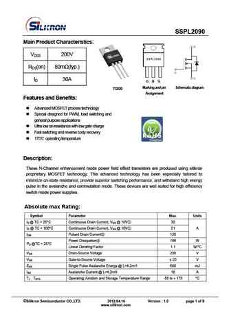
Pd ⓘ - Maximum Power Dissipation: 166 W
|Vds|ⓘ - Maximum Drain-Source Voltage: 200 V
|Vgs|ⓘ - Maximum Gate-Source Voltage: 20 V
|Id| ⓘ - Maximum Drain Current: 30 A
Tj ⓘ - Maximum Junction Temperature: 175 °C
Electrical Characteristics
tr ⓘ - Rise Time: 13.6 nS
Cossⓘ - Output Capacitance: 250 pF
RDSonⓘ - Maximum Drain-Source On-State Resistance: 0.09 Ohm
Package: TO220
SSPL2090 substitution
- MOSFET ⓘ Cross-Reference Search
SSPL2090 datasheet
sspl2090.pdf
SSPL2090 Main Product Characteristics VDSS 200V RDS(on) 80m (typ.) ID 30A Ma r ki ng a nd pin Sche ma ti c di agra m TO220 Assignment Features and Benefits Advanced MOSFET process technology Special designed for PWM, load switching and general purpose applications Ultra low on-resistance with low gate charge Fast switching and reverse body recovery... See More ⇒
sspl2015f.pdf
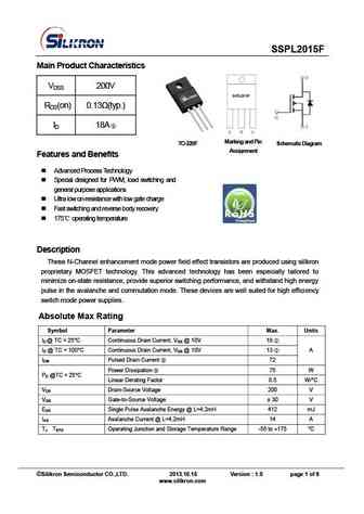
SSPL2015F Main Product Characteristics VDSS 200V RDS(on) 0.13 (typ.) ID 18A Marking and P in Schematic Diagram TO-220F Assignment Features and Benefits Advanced Process Technology Special designed for PWM, load switching and general purpose applications Ultra low on-resistance with low gate charge Fast switching and reverse body recovery 17... See More ⇒
sspl2015d.pdf
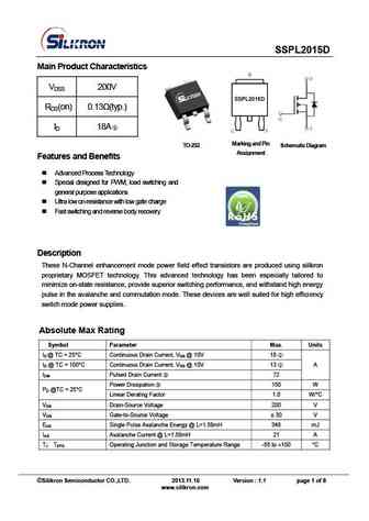
SSPL2015D Main Product Characteristics VDSS 200V RDS(on) 0.13 (typ.) ID 18A Schematic Diagram TO-252 Marking a nd P in Assignment Features and Benefits Advanced Process Technology Special designed for PWM, load switching and general purpose applications Ultra low on-resistance with low gate charge Fast switching and reverse body recovery Descri... See More ⇒
sspl2015.pdf
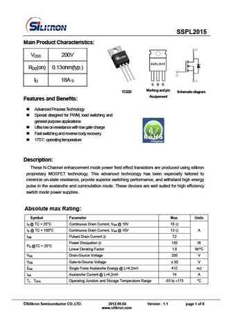
SSPL2015 Main Product Characteristics VDSS 200V RDS(on) 0.13ohm(typ.) ID 18A Mar ki ng a nd p in Sche ma ti c di agr a m TO220 Assignment Features and Benefits Advanced Process Technology Special designed for PWM, load switching and general purpose applications Ultra low on-resistance with low gate charge Fast switching and reverse body recovery... See More ⇒
Detailed specifications: SSFT4004, SSPL1010, SSPL1022, SSPL1042, SSPL1090, SSPL2015, SSPL2015D, SSPL2015F, 7N60, SSPL4004, SSPL50N30H, SSPL5505, SSPL5508, MMBT7002, MMBT7002DW, MMBT7002E, MMBT7002K
Keywords - SSPL2090 MOSFET specs
SSPL2090 cross reference
SSPL2090 equivalent finder
SSPL2090 pdf lookup
SSPL2090 substitution
SSPL2090 replacement
Can't find your MOSFET? Learn how to find a substitute transistor by analyzing voltage, current and package compatibility
🌐 : EN ES РУ
LIST
Last Update
MOSFET: FTF30P35D | FTF25N35DHVT | FTF15N35D | FTE15C35G | FTP02P15G | FTE02P15G | AKF30N5P0SX | AKF30N10S | AKF20P45D | CM4407
Popular searches
2sc1775 datasheet | j377 transistor datasheet | svt20240nt | tip41c replacement | b772m transistor | mj15003g datasheet | irfp460n datasheet | mj15025g


