P2610BT Specs and Replacement
Type Designator: P2610BT
Type of Transistor: MOSFET
Type of Control Channel: N-Channel
Absolute Maximum Ratings
Pd ⓘ - Maximum Power Dissipation: 83 W
|Vds|ⓘ - Maximum Drain-Source Voltage: 100 V
|Vgs|ⓘ - Maximum Gate-Source Voltage: 20 V
|Id| ⓘ - Maximum Drain Current: 36 A
Tj ⓘ - Maximum Junction Temperature: 150 °C
Electrical Characteristics
tr ⓘ - Rise Time: 43 nS
Cossⓘ - Output Capacitance: 148 pF
RDSonⓘ - Maximum Drain-Source On-State Resistance: 0.0268 Ohm
Package: TO220
P2610BT substitution
- MOSFET ⓘ Cross-Reference Search
P2610BT datasheet
p2610bt.pdf
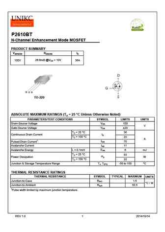
P2610BT N-Channel Enhancement Mode MOSFET PRODUCT SUMMARY V(BR)DSS RDS(ON) ID 26.8m @VGS = 10V 100V 36A TO-220 ABSOLUTE MAXIMUM RATINGS (TA = 25 C Unless Otherwise Noted) PARAMETERS/TEST CONDITIONS SYMBOL LIMITS UNITS VDS Drain-Source Voltage 100 V VGS Gate-Source Voltage 20 TC = 25 C 36 ID Continuous Drain Current TC = 100 C 23 A IDM 70 Pulsed Drain Curre... See More ⇒
p2610bt.pdf
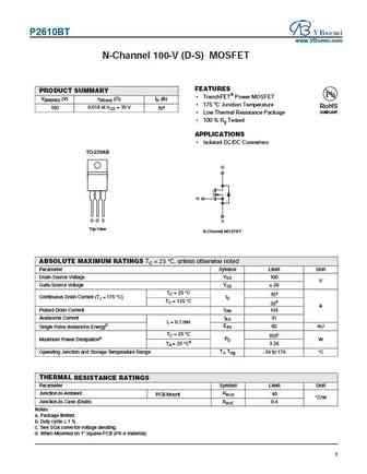
P2610BT www.VBsemi.com N-Channel 100-V (D-S) MOSFET FEATURES PRODUCT SUMMARY TrenchFET Power MOSFET V(BR)DSS (V) rDS(on) ( )ID (A) 175 C Junction Temperature RoHS 0.018 at VGS = 10 V 100 70a COMPLIANT Low Thermal Resistance Package 100 % Rg Tested APPLICATIONS Isolated DC/DC Converters TO-220AB D G G D S S Top View N-Channel MOSFET ABSOLUTE MA... See More ⇒
p2610btf.pdf
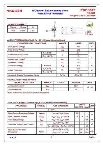
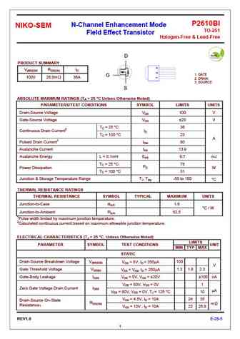
P2610BTF N-Channel Enhancement Mode NIKO-SEM TO-220F Field Effect Transistor Halogen-Free & Lead-Free D PRODUCT SUMMARY V(BR)DSS RDS(ON) ID 100V 26.8m 24A G 1 GATE 2 DRAIN 3 SOURCE S ABSOLUTE MAXIMUM RATINGS (TA = 25 C Unless Otherwise Noted) PARAMETERS/TEST CONDITIONS SYMBOL LIMITS UNITS Drain-Source Voltage VDS 100 V Gate-Source Voltage VGS 20 V T... See More ⇒
p2610bs.pdf
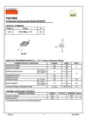
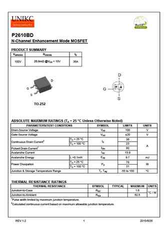
P2610BS N-Channel Enhancement Mode MOSFET PRODUCT SUMMARY V(BR)DSS RDS(ON) ID 26.8m @VGS = 10V 100V 36A TO-263 ABSOLUTE MAXIMUM RATINGS (TA = 25 C Unless Otherwise Noted) PARAMETERS/TEST CONDITIONS SYMBOL LIMITS UNITS VDS Drain-Source Voltage 100 V VGS Gate-Source Voltage 20 TC = 25 C 36 ID Continuous Drain Current TC = 100 C 23 A IDM 70 Pulsed Drain Curr... See More ⇒
Detailed specifications: P1610AT, P1703BDG, P2610ADG, P2610AI, P2610ATFG, P2610ATG, P2610BD, P2610BS, IRF9540N, P2615ATFG, P2615ATG, P261AFEA, P261ALV, P1810ATX, P1820AD, P1820BD, P1825AD
Keywords - P2610BT MOSFET specs
P2610BT cross reference
P2610BT equivalent finder
P2610BT pdf lookup
P2610BT substitution
P2610BT replacement
Need a MOSFET replacement? Our guide shows you how to find a perfect substitute by comparing key parameters and specs
