P3710BD Datasheet. Specs and Replacement
Type Designator: P3710BD 📄📄
Type of Transistor: MOSFET
Type of Control Channel: N-Channel
Absolute Maximum Ratings
Pd ⓘ - Maximum Power Dissipation: 50 W
|Vds|ⓘ - Maximum Drain-Source Voltage: 100 V
|Vgs|ⓘ - Maximum Gate-Source Voltage: 20 V
|Id| ⓘ - Maximum Drain Current: 25 A
Tj ⓘ - Maximum Junction Temperature: 150 °C
Electrical Characteristics
tr ⓘ - Rise Time: 2 nS
Cossⓘ - Output Capacitance: 127 pF
RDSonⓘ - Maximum Drain-Source On-State Resistance: 0.037 Ohm
Package: TO252
📄📄 Copy
P3710BD substitution
- MOSFET ⓘ Cross-Reference Search
P3710BD datasheet
p3710bd.pdf
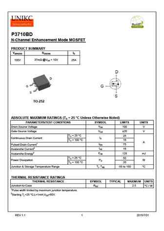
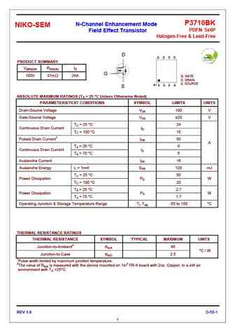
P3710BD N-Channel Enhancement Mode MOSFET PRODUCT SUMMARY V(BR)DSS RDS(ON) ID 37m @VGS = 10V 100V 25A TO-252 ABSOLUTE MAXIMUM RATINGS (TA = 25 C Unless Otherwise Noted) PARAMETERS/TEST CONDITIONS SYMBOL LIMITS UNITS VDS Drain-Source Voltage 100 V VGS Gate-Source Voltage 20 V TC = 25 C 25 ID Continuous Drain Current TC = 100 C 16 A IDM 75 Pulsed Drain Curren... See More ⇒
p3710bd.pdf
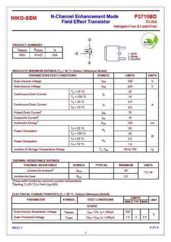
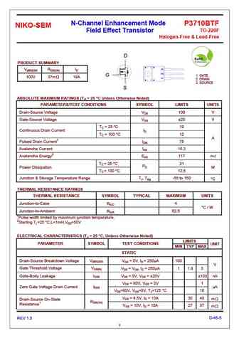
N-Channel Enhancement Mode P3710BD NIKO-SEM TO-252 Field Effect Transistor Halogen-Free & Lead-Free D PRODUCT SUMMARY V(BR)DSS RDS(ON) ID 1. GATE G 100V 37m 25A 2. DRAIN 3. SOURCE S ABSOLUTE MAXIMUM RATINGS (TA = 25 C Unless Otherwise Noted) PARAMETERS/TEST CONDITIONS SYMBOL LIMITS UNITS Drain-Source Voltage VDS 100 V Gate-Source Voltage VGS 20 V TC = 2... See More ⇒
p3710bv.pdf
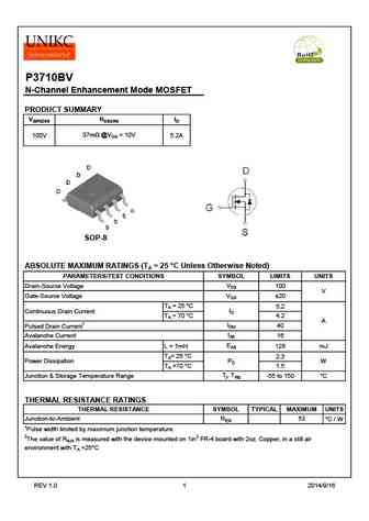
P3710BV N-Channel Enhancement Mode MOSFET PRODUCT SUMMARY V(BR)DSS RDS(ON) ID 37m @VGS = 10V 100V 5.2A SOP-8 ABSOLUTE MAXIMUM RATINGS (TA = 25 C Unless Otherwise Noted) PARAMETERS/TEST CONDITIONS SYMBOL LIMITS UNITS VDS Drain-Source Voltage 100 V VGS Gate-Source Voltage 20 TA = 25 C 5.2 ID Continuous Drain Current TA = 70 C 4.2 A IDM 40 Pulsed Drain Curren... See More ⇒
p3710bt.pdf
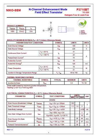
N-Channel Enhancement Mode P3710BT NIKO-SEM TO-220 Field Effect Transistor Halogen-Free & Lead-Free D PRODUCT SUMMARY V(BR)DSS RDS(ON) ID G 1. GATE 100V 37m 31A 2. DRAIN 3. SOURCE S ABSOLUTE MAXIMUM RATINGS (TA = 25 C Unless Otherwise Noted) PARAMETERS/TEST CONDITIONS SYMBOL LIMITS UNITS Drain-Source Voltage VDS 100 V Gate-Source Voltage VGS 20 V TC = 25 C 3... See More ⇒

Detailed specifications: P3202CMG, P3203CMG, P3203EVG, P3204HV, P3304EV, P3304QV, P3503EVG, P3710AV, IRFB4115, P3710BV, PZ0703ED, PZ0703EK, PZ0703EV, PZ1003EK, PZ1203EV, PZ2003EEA, PZ2003EV
Keywords - P3710BD MOSFET specs
P3710BD cross reference
P3710BD equivalent finder
P3710BD pdf lookup
P3710BD substitution
P3710BD replacement
Need a MOSFET replacement? Our guide shows you how to find a perfect substitute by comparing key parameters and specs
