4953A Specs and Replacement
Type Designator: 4953A
Type of Transistor: MOSFET
Type of Control Channel: P-Channel
Absolute Maximum Ratings
Pd ⓘ
- Maximum Power Dissipation: 2 W
|Vds|ⓘ - Maximum Drain-Source Voltage: 30 V
|Vgs|ⓘ - Maximum Gate-Source Voltage: 20 V
|Id| ⓘ - Maximum Drain Current: 5.3 A
Tj ⓘ - Maximum Junction Temperature: 175 °C
Electrical Characteristics
RDSonⓘ - Maximum Drain-Source On-State Resistance: 0.06 Ohm
Package: SOP8
- MOSFET ⓘ Cross-Reference Search
4953A datasheet
..1. Size:1799K shenzhen
4953a.pdf 
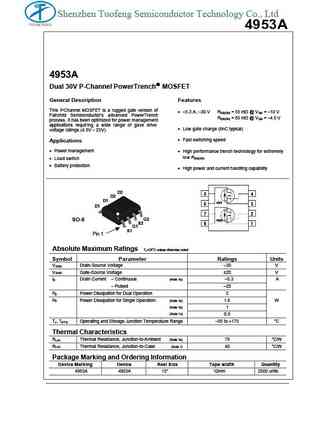
Shenzhen Tuofeng Semiconductor Technology Co., Ltd 4953A 4953A Dual 30V P-Channel PowerTrench MOSFET General Description Features This P MOSFET is a rugged gate version of -Channel 5.3 A, 30 V R = 55 m @ V = 10 V DS(ON) GS Fairchild Semiconductor s advanced PowerTrench R = 85 m @ V = 4.5 V DS(ON) GS process. It has been optimized for power managemen... See More ⇒
0.1. Size:242K vishay
si4953ady.pdf
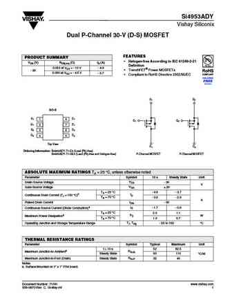
Si4953ADY Vishay Siliconix Dual P-Channel 30-V (D-S) MOSFET FEATURES PRODUCT SUMMARY Halogen-free According to IEC 61249-2-21 VDS (V) RDS(on) ( )ID (A) Definition 0.053 at VGS = - 10 V - 4.9 TrenchFET Power MOSFETs - 30 0.090 at VGS = - 4.5 V - 3.7 Compliant to RoHS Directive 2002/95/EC S1 S2 SO-8 S1 1 D1 8 G1 G2 G1 2 D1 7 S2 3 D2 6 G2 4 D2 5 To... See More ⇒
0.2. Size:526K cet
cem4953a.pdf
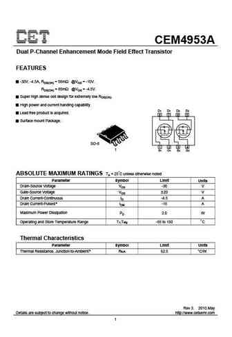
CEM4953A Dual P-Channel Enhancement Mode Field Effect Transistor FEATURES -30V, -4.5A, RDS(ON) = 58m @VGS = -10V. RDS(ON) = 85m @VGS = -4.5V. Super high dense cell design for extremely low RDS(ON). High power and current handing capability. D1 D1 D2 D2 Lead free product is acquired. 8 7 6 5 Surface mount Package. SO-8 1 2 3 4 1 S1 G1 S2 G2 ABSOLUTE MAXIMUM RATINGS TA = 25 ... See More ⇒
0.3. Size:1498K kexin
si4953ady.pdf
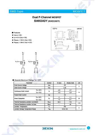
SMD Type MOSFET Dual P-Channel MOSFET SI4953ADY (KI4953ADY) SOP-8 Unit mm Features VDS (V) =-30V ID =-4.9 A (VGS =-10V) 1.50 0.15 RDS(ON) 53m (VGS =-10V) RDS(ON) 90m (VGS =-4.5V) 1 S1 5 D2 6 D2 2 G1 7 D1 3 S2 8 D1 4 G2 S1 S2 G1 G2 D1 D1 D2 D2 Absolute Maximum Ratings Ta = 25 Parameter Symbol 10 secs Steady State Unit Drain-Sourc... See More ⇒
0.4. Size:273K belling
blm4953a.pdf
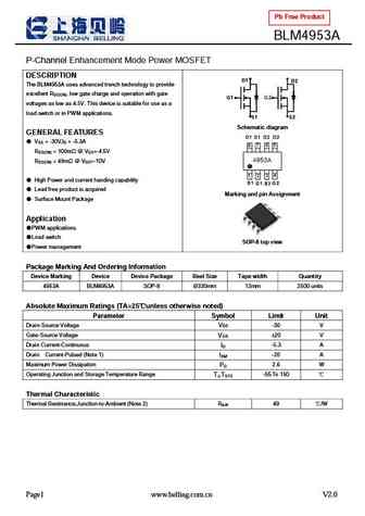
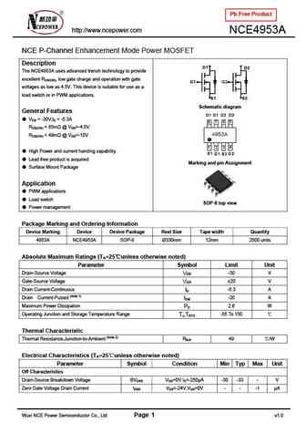
Pb Free Product BLM4953A P-Channel Enhancement Mode Power MOSFET DESCRIPTION D1 D2 The BLM4953A uses advanced trench technology to provide excellent R , low gate charge and operation with gate DS(ON) G1 G2 voltages as low as 4.5V. This device is suitable for use as a load switch or in PWM applications. S1 S2 Schematic diagram GENERAL FEATURES V = -30V,I = -5.3A DS... See More ⇒
0.6. Size:415K prospower
ps4953a.pdf
PS4953A 30V Dual Channel PMOSEFT Revision 1.0 Update Date Apr. 2011 ProsPower Microelectronics Co., Ltd PS4953A 30V Dual Channel PMOSFET 2. Applications 1. General Description PWM applications The PS4953A uses advanced trench technology Load switch and design to provide excellent Rds(on) with low Power management gate charge and operation with gate voltages as ... See More ⇒
0.7. Size:386K semtron
stp4953a.pdf
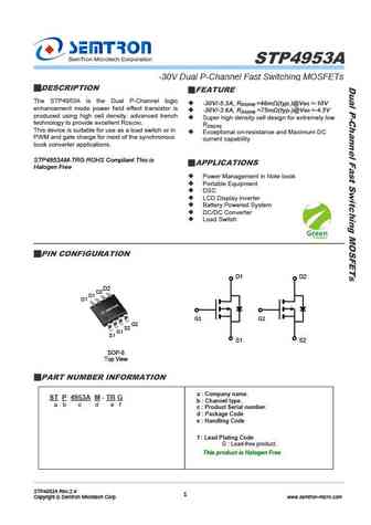
STP4953A -30V Dual P-Channel Fast Switching MOSFETs DESCRIPTION FEATURE The STP4953A is the Dual P-Channel logic -30V/-5.3A, RDS(ON) =46m (typ.)@VGS =-10V enhancement mode power field effect transistor is -30V/-3.6A, RDS(ON) =75m (typ.)@VGS =-4.5V produced using high cell density. advanced trench Super high density cell design for extremely low technology ... See More ⇒
0.9. Size:577K jiejie micro
jmtp4953a.pdf
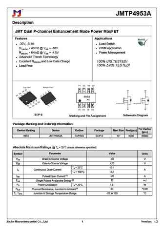
JMTP4953A Description JMT Dual P-channel Enhancement Mode Power MosFET Features Applications -30V, -5.1A Load Switch RDS(ON) ... See More ⇒
0.10. Size:1300K winsok
wsp4953a.pdf
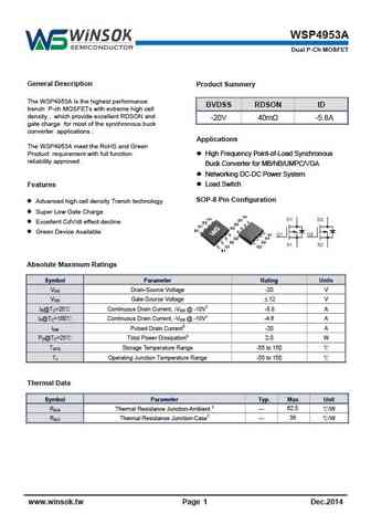
WSP4953A Dual P-Ch MOSFET General Description Product Summery The WSP4953A is the highest performance BVDSS RDSON ID trench P-ch MOSFETs with extreme high cell density , which provide excellent RDSON and -20V 40m -5.8A gate charge for most of the synchronous buck converter applications . Applications The WSP4953A meet the RoHS and Green Product requirement with full fu... See More ⇒
0.11. Size:864K cn vbsemi
si4953ady-t1-e3.pdf
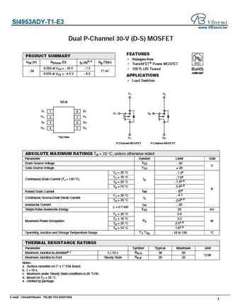
SI4953ADY-T1-E3 www.VBsemi.tw Dual P-Channel 30-V (D-S) MOSFET FEATURES PRODUCT SUMMARY Halogen-free VDS (V) RDS(on) ( ) ID (A)d, e Qg (Typ.) TrenchFET Power MOSFET 0.029 at VGS = - 10 V - 7.3 100 % UIS Tested RoHS - 30 17 nC COMPLIANT 0.039 at VGS = - 4.5 V - 6.3 APPLICATIONS Load Switches S1 S2 SO-8 S1 1 D1 8 G1 G2 G1 2 D1 7 S2 3 D2 6 G2 4 D2 5 ... See More ⇒
0.12. Size:929K cn vbsemi
sdm4953a.pdf
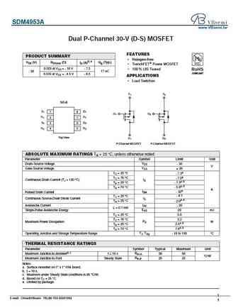
SDM4953A www.VBsemi.tw Dual P-Channel 30-V (D-S) MOSFET FEATURES PRODUCT SUMMARY Halogen-free VDS (V) RDS(on) ( ) ID (A)d, e Qg (Typ.) TrenchFET Power MOSFET 0.029 at VGS = - 10 V - 7.3 100 % UIS Tested RoHS - 30 17 nC COMPLIANT 0.039 at VGS = - 4.5 V - 6.3 APPLICATIONS Load Switches S1 S2 SO-8 S1 1 D1 8 G1 G2 G1 2 D1 7 S2 3 D2 6 G2 4 D2 5 Top Vie... See More ⇒
0.13. Size:1679K cn vbsemi
vbza4953a.pdf
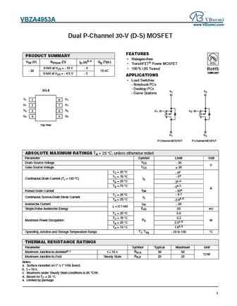
VBZA4953A www.VBsemi.com Dual P-Channel 30-V (D-S) MOSFET FEATURES PRODUCT SUMMARY Halogen-free VDS (V) RDS(on) ( ) ID (A)d, e Qg (Typ.) TrenchFET Power MOSFET 0.040 at VGS = - 10 V - 6 100 % UIS Tested RoHS - 30 15 nC COMPLIANT 0.048 at VGS = - 4.5 V - 5 APPLICATIONS Load Switches - Notebook PCs - Desktop PCs SO-8 S1 S2 - Game Stations S1 1 D1 8 G1 2... See More ⇒
0.14. Size:579K cn hmsemi
hm4953a.pdf
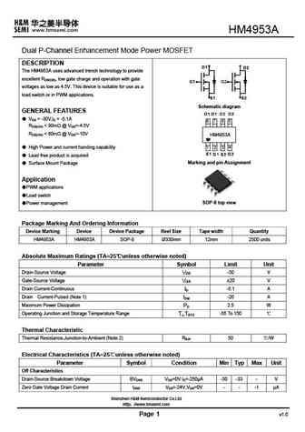
HM4953A Dual P-Channel Enhancement Mode Power MOSFET DESCRIPTION D1 D2 The HM4953A uses advanced trench technology to provide excellent RDS(ON), low gate charge and operation with gate G1 G2 voltages as low as 4.5V. This device is suitable for use as a load switch or in PWM applications. S1 S2 Schematic diagram GENERAL FEATURES VDS = -30V,ID = -5.1A RDS(ON) ... See More ⇒
0.15. Size:1489K cn apm
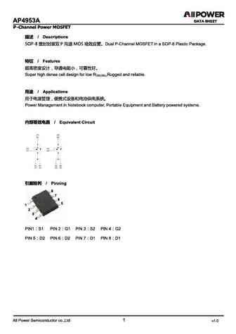
ap4953a.pdf
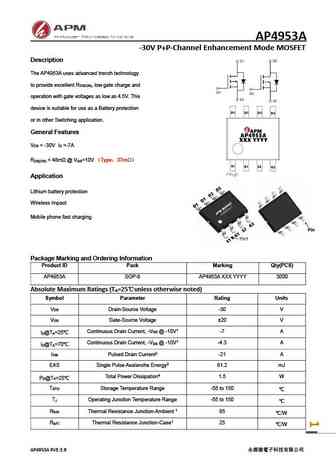
AP4953A -30V P+P-Channel Enhancement Mode MOSFET Description The AP4953A uses advanced trench technology to provide excellent R , low gate charge and DS(ON) operation with gate voltages as low as 4.5V. This device is suitable for use as a Battery protection or in other Switching application. General Features V = -30V I =-7A DS D R ... See More ⇒
Detailed specifications: 4920
, 4946
, 4953
, 6604
, 8810
, 8820
, 8822
, 9435
, IRF530
, 4953B
, 9926A
, 9926B
, AO3410
, APM2317
, FDMA905
, FDN338
, S8205A
.
History: 4835
| NCE65T360
Keywords - 4953A MOSFET specs
4953A cross reference
4953A equivalent finder
4953A pdf lookup
4953A substitution
4953A replacement
Can't find your MOSFET?
Learn how to find a substitute transistor by analyzing voltage, current and package compatibility