60N03 Specs and Replacement
Type Designator: 60N03
Type of Transistor: MOSFET
Type of Control Channel: N-Channel
Absolute Maximum Ratings
Pd ⓘ - Maximum Power Dissipation: 75 W
|Vds|ⓘ - Maximum Drain-Source Voltage: 30 V
|Vgs|ⓘ - Maximum Gate-Source Voltage: 20 V
|Id| ⓘ - Maximum Drain Current: 60 A
Tj ⓘ - Maximum Junction Temperature: 150 °C
Electrical Characteristics
RDSonⓘ - Maximum Drain-Source On-State Resistance: 0.009 Ohm
60N03 substitution
- MOSFET ⓘ Cross-Reference Search
60N03 datasheet
60n03.pdf
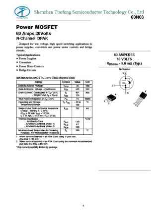
Shenzhen Tuofeng Semiconductor Technology Co., Ltd 60N03 Power MOSFET 60 Amps,30Volts N-Channel DPAK Designed for low voltage, high speed switching applications in power supplies, converters and power motor controls and bridge circuits. Typical Applications 60 AMPERES Power Supplies 30 VOLTS Converters RDS(on) = 9.0 mW (Typ.) Power Motor Controls N-Channel Bridge... See More ⇒
msk60n03df.pdf
www.msksemi.com MSK60N03DF Semiconductor Compiance Description The MSK60N03DF uses advanced trench technology D D D D to provide excellent RDS(ON), low gate charge and operation with gate voltages as low as 4.5V. This device is suitable for use as a S S S G Battery protection or in other Switching application. General Features DFN3X3-8L VDS = 30V ID =60 A RDS(ON) ... See More ⇒
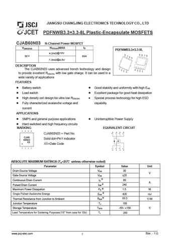
cjab60n03.pdf
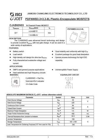
JIANGSU CHANGJING ELECTRONICS TECHNOLOGY CO., LTD PDFNWB3.3 3.3-8L Plastic-Encapsulate MOSFETS CJAB60N03 N-Channel Power MOSFET ID V(BR)DSS RDS(on)MAX PDFNWB3.3 3.3-8L 4.2m @10V 30 V 60A 7.3m @4.5V DESCRIPTION The CJAB60N03 uses advanced trench technology and design to provide excellent RDS(ON) with low gate charge. It can be used in a wide variety of applications FEA... See More ⇒
phb160n03t-01.pdf
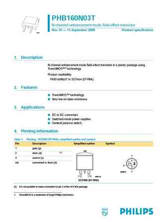
PHB160N03T N-channel enhancement mode field-effect transistor Rev. 01 13 September 2000 Product specification M3D166 1. Description N-channel enhancement mode field-effect transistor in a plastic package using TrenchMOS 1 technology. Product availability PHB160N03T in SOT404 (D2-PAK). 2. Features TrenchMOS technology Very low on-state resistance. 3. Applications DC to ... See More ⇒
stb60n03l-10.pdf
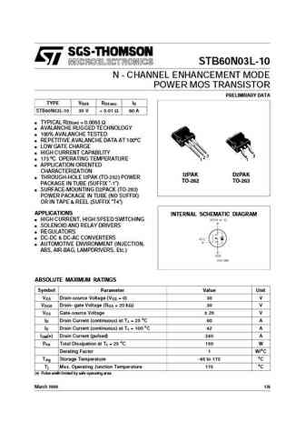
STB60N03L-10 N - CHANNEL ENHANCEMENT MODE POWER MOS TRANSISTOR PRELIMIRARY DATA TYPE V R I DSS DS(on) D STB60N03L-10 30 V ... See More ⇒
np60n03sug.pdf

To our customers, Old Company Name in Catalogs and Other Documents On April 1st, 2010, NEC Electronics Corporation merged with Renesas Technology Corporation, and Renesas Electronics Corporation took over all the business of both companies. Therefore, although the old company name remains in this document, it is a valid Renesas Electronics document. We appreciate your understanding. ... See More ⇒
np60n03kug.pdf
To our customers, Old Company Name in Catalogs and Other Documents On April 1st, 2010, NEC Electronics Corporation merged with Renesas Technology Corporation, and Renesas Electronics Corporation took over all the business of both companies. Therefore, although the old company name remains in this document, it is a valid Renesas Electronics document. We appreciate your understanding. ... See More ⇒
fqb60n03l.pdf
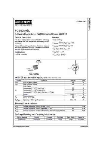
October 2002 FQB60N03L N-Channel Logic Level PWM Optimized Power MOSFET General Description Features This device employs a new advanced MOSFET technology Fast switching and features low gate charge while maintaining low on- rDS(ON) = 0.010 (Typ), VGS = 10V resistance. rDS(ON) = 0.017 (Typ), VGS = 5V Optimized for switching applications, this device improves the overa... See More ⇒
ipd060n03lg ipf060n03lg ips060n03lg ipu060n03lg.pdf

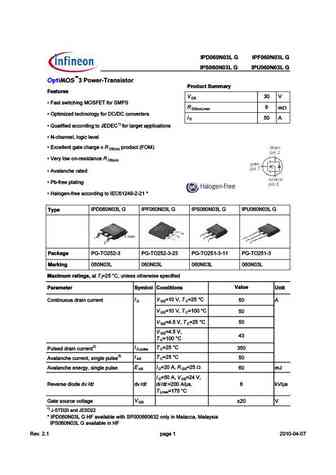
Type IPD060N03L G IPF060N03L G IPS060N03L G IPU060N03L G OptiMOS 3 Power-Transistor Product Summary Features V 30 V DS Fast switching MOSFET for SMPS R 6 m DS(on),max Optimized technology for DC/DC converters I 50 A D Qualified according to JEDEC1) for target applications N-channel, logic level Excellent gate charge x R product (FOM) DS(on) Very lo... See More ⇒
ipd060n03lg .pdf
pe % # ! % # ! %' # ! %) # ! % (>.;?6?@ %>E Features D S !4EF EI... See More ⇒
ips060n03l.pdf

pe % # ! % # ! %' # ! %) # ! % (>.;?6?@ %>E Features D S !4EF EI... See More ⇒
ipd060n03l ipf060n03l ips060n03l ipu060n03l.pdf
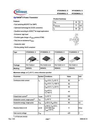
Type IPD060N03L G IPF060N03L G IPS060N03L G IPU060N03L G OptiMOS 3 Power-Transistor Product Summary Features V 30 V DS Fast switching MOSFET for SMPS R 6 m DS(on),max Optimized technology for DC/DC converters I 50 A D Qualified according to JEDEC1) for target applications N-channel, logic level Excellent gate charge x R product (FOM) DS(on) Very low... See More ⇒
ipd060n03lg.pdf
pe % # ! % # ! %' # ! %) # ! % (>.;?6?@ %>E Features D R 3DE DH;E5 ;@9 ') - . 8AC -'*- mW D n) m x R ) BE;?;K76 E75 @A>A9J 8AC 5A@G7CE7CD D 1) R + F3>;8;76 355AC6;@9 EA $ 8AC E3C97E 3BB>;53E;A@D R ( 5 3@@7> >A9;5 >7G7> R I57>>7@E 93E7 5 3C97 I BCA6F5E ) ' D n) R 07CJ >AH A@ C7D;DE3@57 D n) R G3>3@5 7 C3E76 R *4 8C77 B>3E;@9 Type #* ( & ! #* ( & ! #*... See More ⇒
ipd060n03l.pdf
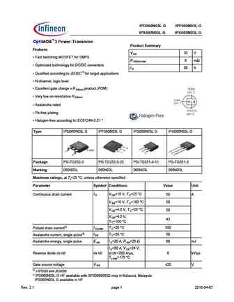
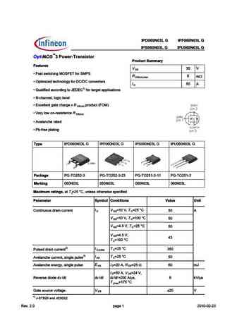
Type IPD060N03L G IPF060N03L G IPS060N03L G IPU060N03L G OptiMOS 3 Power-Transistor Product Summary Features V 30 V DS Fast switching MOSFET for SMPS R 6 m DS(on),max Optimized technology for DC/DC converters I 50 A D Qualified according to JEDEC1) for target applications N-channel, logic level Excellent gate charge x R product (FOM) DS(on) Very lo... See More ⇒
ntd60n03-001.pdf
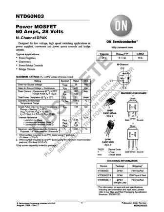
NTD60N03 Power MOSFET 60 Amps, 28 Volts N-Channel DPAK Designed for low voltage, high speed switching applications in power supplies, converters and power motor controls and bridge http //onsemi.com circuits. V(BR)DSS RDS(on) TYP ID MAX Typical Applications 28 V 6.1 mW 60 A Power Supplies Converters N-Channel Power Motor Controls D Bridge Circuits MAXIMUM RATING... See More ⇒
ut60n03.pdf
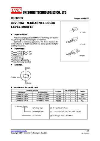
UNISONIC TECHNOLOGIES CO., LTD UT60N03 Power MOSFET 30V, 60A N-CHANNEL LOGIC LEVEL MOSFET 1 TO-252 DESCRIPTION This device employs advanced MOSFET technology and features low gate charge while maintaining low on-resistance. Optimized for switching applications, this device improves the 1 overall efficiency of DC/DC converters and allows operation to higher TO-251 switchi... See More ⇒
ut60n03l-ta3-t ut60n03g-ta3-t ut60n03l-tm3-t ut60n03g-tm3-t ut60n03l-tn3-r ut60n03g-tn3-r ut60n03l-tnd-r ut60n03g-tnd-r.pdf
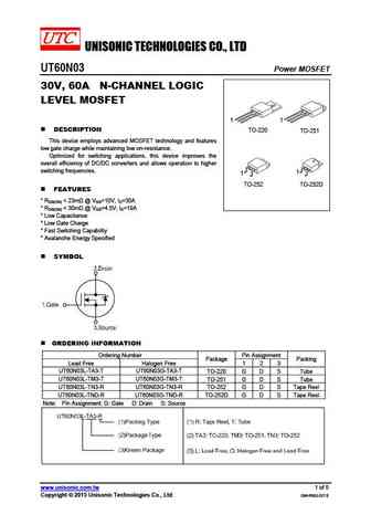
UNISONIC TECHNOLOGIES CO., LTD UT60N03 Power MOSFET 30V, 60A N-CHANNEL LOGIC LEVEL MOSFET 1 1 DESCRIPTION TO-220 TO-251 This device employs advanced MOSFET technology and features low gate charge while maintaining low on-resistance. Optimized for switching applications, this device improves the overall efficiency of DC/DC converters and allows operation to higher switch... See More ⇒
tsm60n03cp.pdf
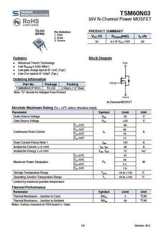
TSM60N03 30V N-Channel Power MOSFET TO-252 PRODUCT SUMMARY Pin Definition (DPAK) 1. Gate VDS (V) RDS(on)(m ) ID (A) 2. Drain 3. Source 30 4.5 @ VGS =10V 60 Features Block Diagram Advanced Trench Technology Low RDS(ON) 4.5m (Max.) Low gate charge typical @ 12nC (Typ.) Low Crss typical @ 140pF (Typ.) Ordering Information Part No. Packag... See More ⇒
cjab60n03.pdf
JIANGSU CHANGJING ELECTRONICS TECHNOLOGY CO., LTD PDFNWB3.3 3.3-8L Plastic-Encapsulate MOSFETS CJAB60N03 N-Channel Power MOSFET ID V(BR)DSS RDS(on)MAX PDFNWB3.3 3.3-8L 4.2m @10V 30 V 60A 7.3m @4.5V DESCRIPTION The CJAB60N03 uses advanced trench technology and design to provide excellent RDS(ON) with low gate charge. It can be used in a wide variety of applications FEA... See More ⇒
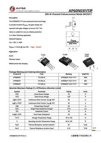
ap60n03gs.pdf
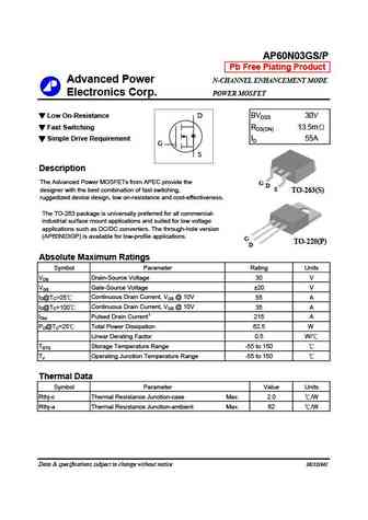
AP60N03GS/P Pb Free Plating Product Advanced Power N-CHANNEL ENHANCEMENT MODE Electronics Corp. POWER MOSFET Low On-Resistance D BVDSS 30V Fast Switching RDS(ON) 13.5m Simple Drive Requirement ID 55A G S Description The Advanced Power MOSFETs from APEC provide the G D designer with the best combination of fast switching,... See More ⇒
ap60n03gp.pdf
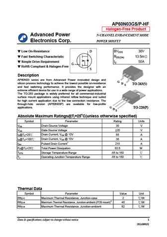
AP60N03GS/P-HF Halogen-Free Product Advanced Power N-CHANNEL ENHANCEMENT MODE Electronics Corp. POWER MOSFET Low On-Resistance D BVDSS 30V Fast Switching Characteristic RDS(ON) 13.5m Simple Drive Requirement ID 55A G RoHS Compliant & Halogen-Free S Description AP60N03 series are from Advanced Power innovated design and G silicon process technology to achieve the l... See More ⇒
ap60n03gh ap60n03gj.pdf
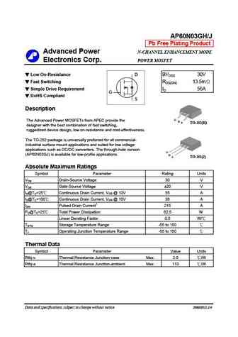
AP60N03GH/J Pb Free Plating Product Advanced Power N-CHANNEL ENHANCEMENT MODE Electronics Corp. POWER MOSFET Low On-Resistance D BVDSS 30V Fast Switching RDS(ON) 13.5m Simple Drive Requirement ID 55A G RoHS Compliant S Description G The Advanced Power MOSFETs from APEC provide the D S TO-252(H) designer with the best combination of fast switching, ruggedized d... See More ⇒
am60n03-09d.pdf
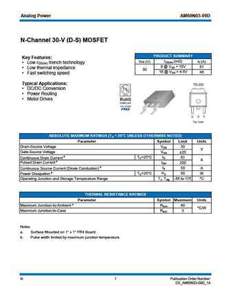
Analog Power AM60N03-09D N-Channel 30-V (D-S) MOSFET PRODUCT SUMMARY Key Features rDS(on) (m ) VDS (V) ID (A) Low r trench technology DS(on) 9 @ VGS = 10V 61 Low thermal impedance 30 16 @ VGS = 4.5V 46 Fast switching speed Typical Applications DC/DC Conversion Power Routing Motor Drives ABSOLUTE MAXIMUM RATINGS (TA = 25 C UNLESS OTHERWISE N... See More ⇒
brcs060n03zc.pdf
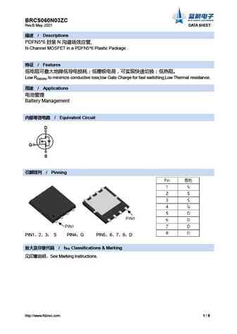
BRCS060N03ZC Rev.B May.-2021 DATA SHEET / Descriptions PDFN5*6 N N-Channel MOSFET in a PDFN5*6 Plastic Package . / Features Low RDS(ON) to minimize conductive loss;low Gate Charge for fast switching;Low Thermal resistance. / Applicat... See More ⇒
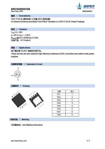
brcs060n03yb.pdf
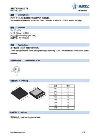
BRCS060N03YB Rev.A Aug.-2021 DATA SHEET / Descriptions PDFN 3 3A-8L N MOS N-Channel Enhancement Mode Field Effect Transistor in a PDFN 3 3A-8L Plastic Package. / Features VDS (V) = 30V ID =40 A (VGS = 20V) RDS(ON)@10V 6mR(Typ.4.7mR) HF Product. / Applications DC/DC ... See More ⇒
brcs060n03dp.pdf
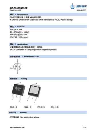
BRCS060N03DP Rev.A Jun.-2022 DATA SHEET / Descriptions TO-252 N MOS N-Channel Enhancement Mode Field Effect Transistor in a TO-252 Plastic Package. / Features VDS (V) = 30V ID =67A (VGS = 20V) RDS(ON)@10V 6mR HF Product. / Applications DC/DC , DC/DC C... See More ⇒
cm60n03c.pdf
R CM60N03C www.jdsemi.cn ShenZhen Jingdao Electronic Co.,Ltd. POWER MOSFET 30V N-Channel Trench-MOS RoHS 1 D/C PM CD W 2 TO-251 TO-252 ... See More ⇒
dh060n03r.pdf
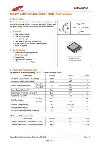
DH060N03R 54A 30V N-channel Enhancement Mode Power MOSFET 1 Description These N-channel enhanced vdmosfets used advanced 2 D V = 30V DSS trench technology design, provided excellent Rdson and low gate charge. Which accords with the RoHS standard. R = 5.3m DS(on) (TYP) G 1 2 Features I = 54A 3 S D Low switching loss Low on resistance Low gate charge Low revers... See More ⇒
me60n03a.pdf
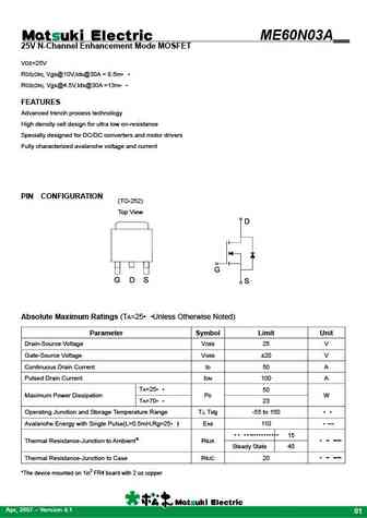
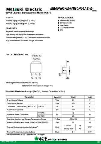
ME60N03A 25V N-Channel Enhancement Mode MOSFET VDS=25V RDS(ON), Vgs@10V,Ids@30A = 8.5m RDS(ON), Vgs@4.5V,Ids@30A =13m FEATURES Advanced trench process technology High density cell design for ultra low on-resistance Specially designed for DC/DC converters and motor drivers Fully characterized avalanche voltage and current PIN CONFIGURATION (TO-252) Top View Absolute ... See More ⇒
me60n03.pdf
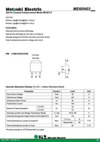
ME60N03 30V N-Channel Enhancement Mode MOSFET VDS=30V RDS(ON), Vgs@10V,Ids@30A = 8.5m RDS(ON), Vgs@4.5V,Ids@20A =13m FEATURES Advanced trench process technology High density cell design for ultra low on-resistance Specially designed for DC/DC converters and motor drivers Fully characterized avalanche voltage and current PIN CONFIGURATION (TO-252) Top View Absolute M... See More ⇒
me60n03 me60n03-g.pdf
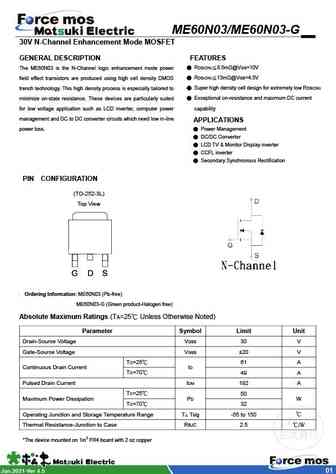
ME60N03/ME60N03-G 30V N-Channel Enhancement Mode MOSFET -g GENERAL DESCRIPTION FEATURES The ME60N03 is the N-Channel logic enhancement mode power RDS(ON) 8.5m @VGS=10V field effect transistors are produced using high cell density DMOS RDS(ON) 13m @VGS=4.5V trench technology. This high density process is especially tailored to Super high density cell design for extre... See More ⇒
me60n03s me60n03s-g.pdf
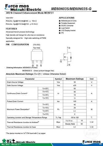
ME60N03S/ME60N03S-G 30V N-Channel Enhancement Mode MOSFET VDS=30V APPLICATIONS Motherboard (V-Core) RDS(ON), Vgs@10V,Ids@30A 10m Portable Equipment RDS(ON), Vgs@4.5V,Ids@15A 18.5m DC/DC Converter Load Switch FEATURES LCD Display inverter Advanced trench process technology IPC High density cell design for ultra low on-resistance Spe... See More ⇒
me60n03as me60n03as-g.pdf
ME60N03AS/ME60N03AS-G 25V N-Channel Enhancement Mode MOSFET VDS=25V APPLICATIONS Motherboard (V-Core) RDS(ON), Vgs@10V,Ids@30A 9m DC/DC Converter RDS(ON), Vgs@ 5V,Ids@15A 18m Load Switch LCD Display inverter FEATURES IPC Advanced trench process technology High density cell design for ultra low on-resistance Specially designed for DC/DC co... See More ⇒
sl160n03r.pdf
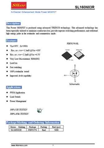
SL160N03R Description This Power MOSFET is produced using advanced TRENCH technology. This advanced technology has been especially tailored to minimize conduction loss, provide superior switching performance, and withstand high energy pulse in the avalanche and commutation mode. Features PDFN5*6-8L V =30V I =160A DS D R = 1.5m @V =10V DS ON TYP GS R ... See More ⇒
hd60n03 hu60n03.pdf
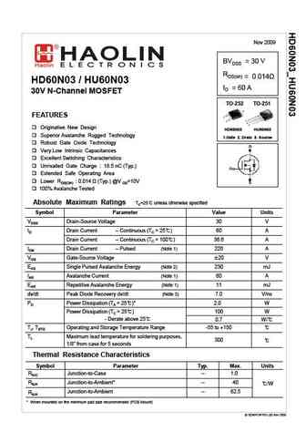
Nov 2009 BVDSS = 30 V RDS(on) = 0.014 HD60N03 / HU60N03 ID = 60 A 30V N-Channel MOSFET TO-252 TO-251 FEATURES Originative New Design HD60N03 HU60N03 Superior Avalanche Rugged Technology 1.Gate 2. Drain 3. Source Robust Gate Oxide Technology Very Low Intrinsic Capacitances Excellent Switching Characteristics Unrivalled Gate Charge 18.5 nC (Typ.) E... See More ⇒
jmtp260n03d.pdf
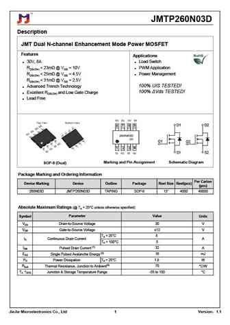
JMTP260N03D Description JMT Dual N-channel Enhancement Mode Power MOSFET Features Applications 30V, 8A Load Switch RDS(ON) ... See More ⇒
hts060n03.pdf
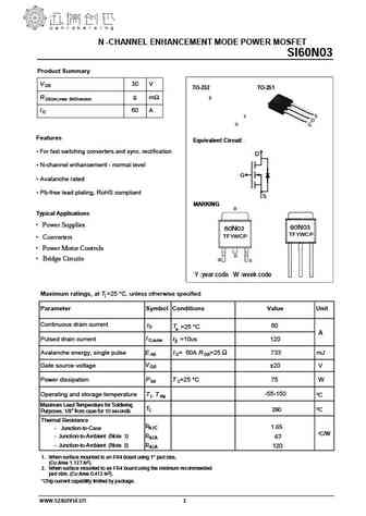
HTS060N03 P-1 30V N-Ch Power MOSFET Feature 30 V VDS High Speed Power Switching, logic level 4.3 RDS(on),typ VGS=10V m Enhanced Body diode dv/dt capability 6.4 RDS(on),typ VGS=4.5V m Enhanced Avalanche Ruggedness 18 A ID 100% UIS Tested, 100% Rg Tested Lead Free Application Synchronous Rectification in SMPS Hard Switching and High Speed Circui... See More ⇒
htm060n03.pdf
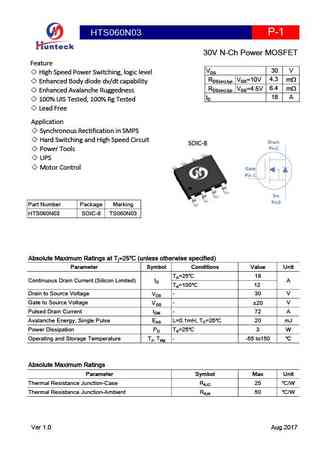
HTM060N03 P-1 30V N-Ch Power MOSFET Feature 30 V VDS High Speed Power Switching, Logic Level 5 RDS(on),typ VGS=10V m Enhanced Avalanche Ruggedness 26 A ID (Sillicon Limited) 100% UIS Tested, 100% Rg Tested Lead Free, Halogen Free Application Hard Switching and High Speed Circuit Drain DFN3x3 DC/DC in Telecoms and Inductrial Gate Src Part Number Pac... See More ⇒
htd060n03.pdf
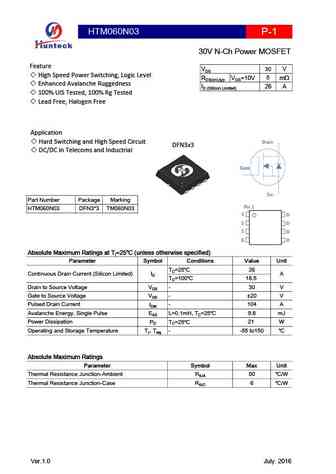
HTD060N03 P-1 30V N-Ch Power MOSFET Feature 30 V VDS High Speed Power Switching, Logic Level 5.3 RDS(on),typ VGS=10V m Enhanced Avalanche Ruggedness 80 A ID (Sillicon Limited) 100% UIS Tested, 100% Rg Tested Lead Free, Halogen Free Application Hard Switching and High Speed Circuit Drain DC/DC in Telecoms and Inductrial TO-252 Gate 2 Src 3 1 Part ... See More ⇒
wsc60n03.pdf
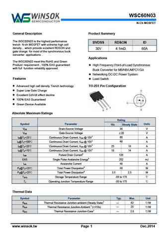
WSC60N03 N-Ch MOSFET General Description Product Summery The WSC60N03 is the highest performance BVDSS RDSON ID trench N-ch MOSFET with extreme high cell density , which provide excellent RDSON and 30V 4.1m 60A gate charge for most of the synchronous buck converter applications . Applications The WSC60N03 meet the RoHS and Green Product requirement , 100% EAS guaranteed ... See More ⇒
vbzfb60n03.pdf
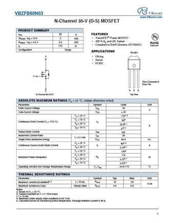
VBZFB60N03 www.VBsemi.com N-Channel 30-V (D-S) MOSFET PRODUCT SUMMARY VDS 30 FEATURES V TrenchFET Power MOSFET RDS(on) VGS = 10 V 2 m 100 % Rg and UIS Tested RDS(on) VGS = 4.5 V 2.4 m Compliant to RoHS Directive 2011/65/EU 110 ID A Configuration Single APPLICATIONS TO-251 D OR-ing Server DC/DC G Drain Connected to Drain-Tab G D S S N-C... See More ⇒
vbzl60n03.pdf
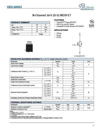
VBZL60N03 www.VBsemi.com N-Channel 30-V (D-S) MOSFET FEATURES TrenchFET Power MOSFET PRODUCT SUMMARY 100 % Rg and UIS Tested VDS 30 V Compliant to RoHS Directive 2011/65/EU RDS(on) VGS = 10 V 12 m RDS(on) VGS = 4.5 V 19 m APPLICATIONS ID 70 A OR-ing D Configuration Single Server DC/DC D2PAK (TO-263) G G D S S N-Channel MOSFET ABSOLUTE ... See More ⇒
vbze60n03.pdf
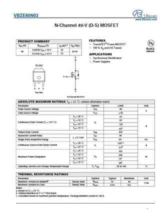
VBZE60N03 www.VBsemi.com N-Channel 40-V (D-S) MOSFET FEATURES PRODUCT SUMMARY TrenchFET Power MOSFET VDS (V) RDS(on) ( ) ID (A)a, c Qg (Typ.) 100 % Rg and UIS Tested RoHS 85 0.007at VGS = 10 V COMPLIANT 40 20 nC 53 0.010at VGS = 4.5 V APPLICATIONS D Synchronous Rectification Power Supplies TO-252 G G D S S Top View N-Channel MOSFET ABSOLUTE MAXIM... See More ⇒
ttd160n03gt ttp160n03gt.pdf
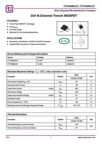
TTD160N03GT, TTP160N03GT Wuxi Unigroup Microelectronics Company 30V N-Channel Trench MOSFET FEATURES Trench Power MOSFET Technology Low RDS(ON) Low Gate Charge Optimized For Fast-switching Applications APPLICATIONS Synchronous Rectification in DC/DC and AC/DC Converters Isolated DC/DC Converters in Telecom and Industrial Device Marking and Package ... See More ⇒
ttg160n03gt.pdf
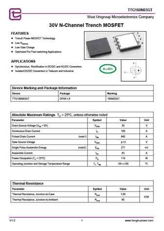
TTG160N03GT Wuxi Unigroup Microelectronics Company 30V N-Channel Trench MOSFET FEATURES Trench Power MOSFET Technology Low RDS(ON) Low Gate Charge Optimized For Fast-switching Applications APPLICATIONS Synchronous Rectification in DC/DC and AC/DC Converters Isolated DC/DC Converters in Telecom and Industrial Device Marking and Package Information ... See More ⇒
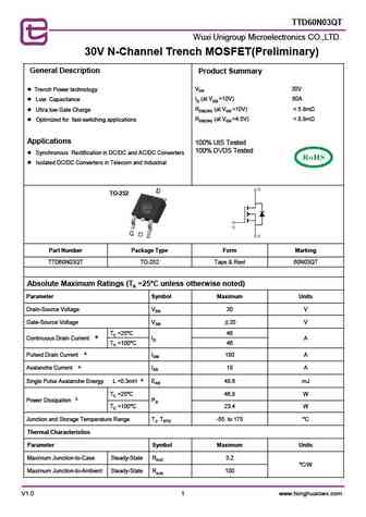
ttd60n03qt.pdf
TTD60N03QT Wuxi Unigroup Microelectronics CO.,LTD. 30V N-Channel Trench MOSFET(Preliminary) General Description Product Summary VDS 30V Trench Power technology ID (at VGS =10V) 60A Low Capacitance RDS(ON) (at VGS =10V) ... See More ⇒
ttg160n03at.pdf
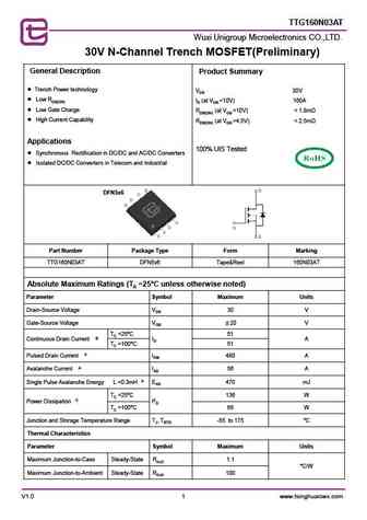
TTG160N03AT Wuxi Unigroup Microelectronics CO.,LTD. 30V N-Channel Trench MOSFET(Preliminary) General Description Product Summary Trench Power technology VDS 30V Low RDS(ON) ID (at VGS =10V) 160A Low Gate Charge RDS(ON) (at VGS =10V) ... See More ⇒
hm60n03d.pdf
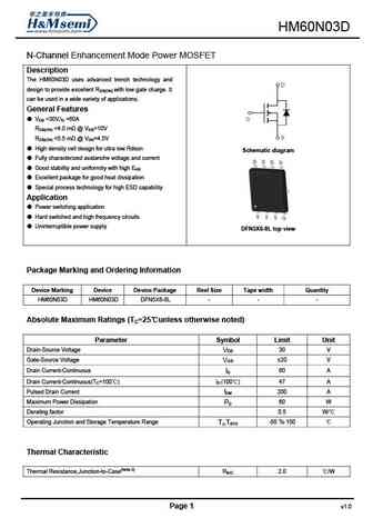
HM60N03D N-Channel Enhancement Mode Power MOSFET Description The HM60N03D uses advanced trench technology and design to provide excellent RDS(ON) with low gate charge. It can be used in a wide variety of applications. General Features VDS =30V,ID =60A RDS(ON) ... See More ⇒
hm60n03.pdf
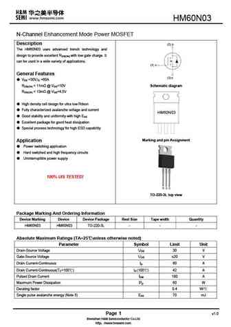
HM60N03 N-Channel Enhancement Mode Power MOSFET Description The HM60N03 uses advanced trench technology and design to provide excellent RDS(ON) with low gate charge. It can be used in a wide variety of applications. General Features VDS =30V,ID =60A RDS(ON) ... See More ⇒
hm60n03k.pdf
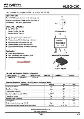
HM60N03K N-Channel Enhancement Mode Power MOSFET DESCRIPTION The HM60N03K uses advanced trench technology and design to provide excellent RDS(ON) with low gate charge. It can be used in a wide variety of applications. GENERAL FEATURES VDS =30V,ID =60A RDS(ON) ... See More ⇒
ipu060n03l.pdf
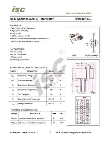
isc N-Channel MOSFET Transistor IPU060N03L FEATURES With TO-251(IPAK) packaging High speed switching Easy to use 100% avalanche tested Minimum Lot-to-Lot variations for robust device performance and reliable operation APPLICATIONS Power supply DC-DC converters Motor control Switching applications ABSOLUTE MAXIMUM RATINGS(T =25 ) a SYMBOL PARAMETER VALUE ... See More ⇒
ipd060n03l.pdf
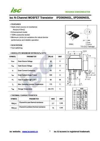
isc N-Channel MOSFET Transistor IPD060N03L, IIPD060N03L FEATURES Static drain-source on-resistance RDS(on) 6m Enhancement mode 100% avalanche tested Minimum Lot-to-Lot variations for robust device performance and reliable operation DESCRITION Fast switching ABSOLUTE MAXIMUM RATINGS(T =25 ) a SYMBOL PARAMETER VALUE UNIT V Drain-Source Voltage 30 V DSS V Ga... See More ⇒
ap60n03d.pdf
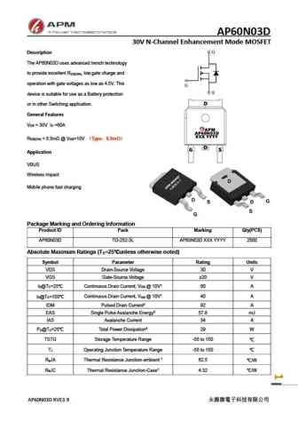
AP60N03D 30V N-Channel Enhancement Mode MOSFET Description The AP60N03D uses advanced trench technology to provide excellent R , low gate charge and DS(ON) operation with gate voltages as low as 4.5V. This device is suitable for use as a Battery protection or in other Switching application. General Features V = 30V I =60A DS D R ... See More ⇒
ap60n03df.pdf
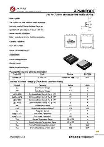
AP60N03DF 30V N-Channel Enhancement Mode MOSFET Description The AP60N03DF uses advanced trench technology to provide excellent R , low gate charge and DS(ON) operation with gate voltages as low as 4.5V. This device is suitable for use as a Battery protection or in other Switching application. General Features V = 30V I =60A DS D R ... See More ⇒
ap60n03nf.pdf
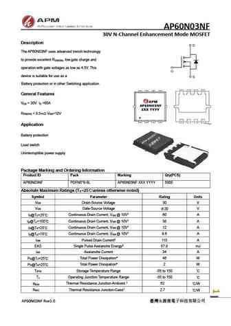
AP60N03NF 30V N-Channel Enhancement Mode MOSFET Description The AP60N03NF uses advanced trench technology to provide excellent R , low gate charge and DS(ON) operation with gate voltages as low as 4.5V. This device is suitable for use as a Battery protection or in other Switching application. General Features V = 30V I =60A DS D R ... See More ⇒
ap60n03p.pdf
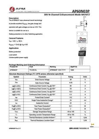
AP60N03P 30V N-Channel Enhancement Mode MOSFET Description The AP60N03P uses advanced trench technology to provide excellent R , low gate charge and DS(ON) operation with gate voltages as low as 4.5V. This device is suitable for use as a Battery protection or in other Switching application. General Features V = 30V I =60 A DS D R ... See More ⇒
ap60n03y.pdf
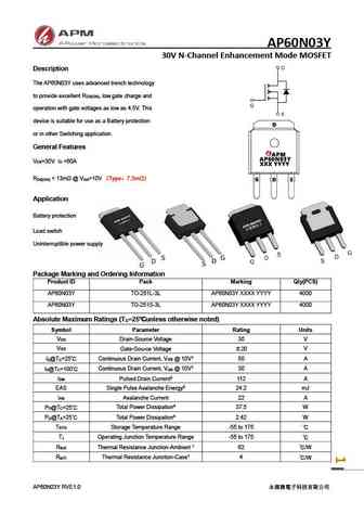
AP60N03Y 30V N-Channel Enhancement Mode MOSFET Description The AP60N03Y uses advanced trench technology to provide excellent R , low gate charge and DS(ON) operation with gate voltages as low as 4.5V. This device is suitable for use as a Battery protection or in other Switching application. General Features V =30V I =60A DS D R ... See More ⇒
Detailed specifications: SI2315 , SI2319 , SI2323 , SI2328 , SIA519 , XP151A13AO , XP152A12CO , 20N06 , AO3400A , 70N03 , 90N03 , SSS10N60 , SSS12N60 , SSS1N60 , SSS2N60 , SSS5N60 , SSS7N60 .
Keywords - 60N03 MOSFET specs
60N03 cross reference
60N03 equivalent finder
60N03 pdf lookup
60N03 substitution
60N03 replacement
Can't find your MOSFET? Learn how to find a substitute transistor by analyzing voltage, current and package compatibility
🌐 : EN ES РУ

LIST
Last Update
MOSFET: ASD80R750E | ASD70R950E | ASD70R600E | ASD70R380E | ASD65R850E | ASD65R550E | ASD65R350E | ASD65R300E | ASD65R280E | ASD65R270E
Popular searches
fr5305 datasheet | y2 transistor | 40n06 | bc108b | oc84 | c6090 | ksa1015yta | 2n4240