3415 Specs and Replacement
Type Designator: 3415
Type of Transistor: MOSFET
Type of Control Channel: P-Channel
Absolute Maximum Ratings
Pd ⓘ - Maximum Power Dissipation: 1.4 W
|Vds|ⓘ - Maximum Drain-Source Voltage: 20 V
|Vgs|ⓘ - Maximum Gate-Source Voltage: 10 V
|Id| ⓘ - Maximum Drain Current: 5.6 A
Tj ⓘ - Maximum Junction Temperature: 150 °C
Electrical Characteristics
tr ⓘ - Rise Time: 10 nS
Cossⓘ - Output Capacitance: 165 pF
RDSonⓘ - Maximum Drain-Source On-State Resistance: 0.045 Ohm
Package: SOT23
3415 substitution
- MOSFET ⓘ Cross-Reference Search
3415 datasheet
irf3415.pdf
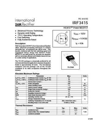
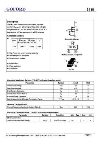
PD - 91477D IRF3415 HEXFET Power MOSFET Advanced Process Technology D Dynamic dv/dt Rating VDSS = 150V 175 C Operating Temperature Fast Switching RDS(on) = 0.042 Fully Avalanche Rated G Description ID = 43A S Fifth Generation HEXFETs from International Rectifier utilize advanced processing techniques to achieve extremely low on-resistance per silicon area. This benef... See More ⇒
auirf3415.pdf
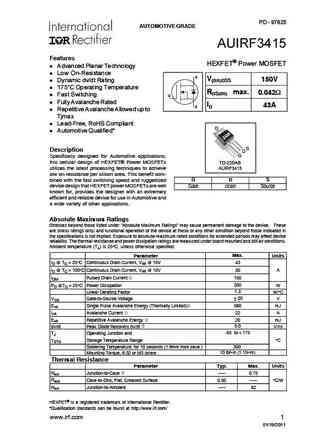
PD - 97625 AUTOMOTIVE GRADE AUIRF3415 Features HEXFET Power MOSFET l Advanced Planar Technology l Low On-Resistance D V(BR)DSS 150V l Dynamic dv/dt Rating l 175 C Operating Temperature RDS(on) max. 0.042 l Fast Switching G l Fully Avalanche Rated ID 43A S l Repetitive Avalanche Allowed up to Tjmax l Lead-Free, RoHS Compliant D l Automotive Qualified* S Descriptio... See More ⇒
irf3415pbf.pdf
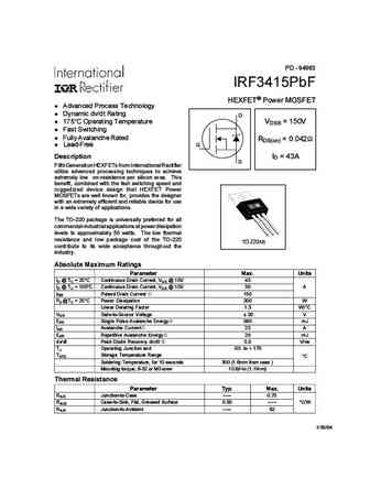
IRF3415PbF l Advanced Process Technology l Dynamic dv/dt Rating D l 175 C Operating Temperature l Fast Switching l Fully Avalanche Rated l Lead-Free G Description S ... See More ⇒
irf3415spbf irf3415lpbf.pdf
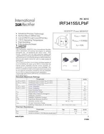
PD - 95112 IRF3415S/LPbF Lead-Free www.irf.com 1 3/16/04 IRF3415S/LPbF 2 www.irf.com IRF3415S/LPbF www.irf.com 3 IRF3415S/LPbF 4 www.irf.com IRF3415S/LPbF www.irf.com 5 IRF3415S/LPbF 6 www.irf.com IRF3415S/LPbF www.irf.com 7 IRF3415S/LPbF D2Pak Package Outline Dimensions are shown in millimeters (inches) D2Pak Part Marking Information (Lead-Free) I I I I I I ... See More ⇒
irf5m3415.pdf
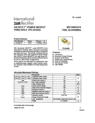
PD - 94286A HEXFET POWER MOSFET IRF5M3415 THRU-HOLE (TO-254AA) 150V, N-CHANNEL Product Summary Part Number BVDSS RDS(on) ID 150V 0.049 35A IRF5M3415 Fifth Generation HEXFET power MOSFETs from TO-254AA International Rectifier utilize advanced processing techniques to achieve the lowest possible on-resistance Features per silicon unit area. This benefit, combined with the ... See More ⇒
irf3415s.pdf
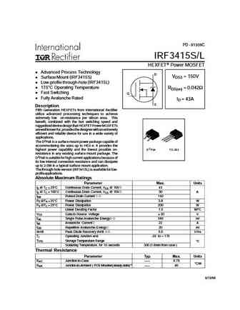
PD - 91509C IRF3415S/L HEXFET Power MOSFET Advanced Process Technology D VDSS = 150V Surface Mount (IRF3415S) Low-profile through-hole (IRF3415L) 175 C Operating Temperature RDS(on) = 0.042 Fast Switching G Fully Avalanche Rated ID = 43A S Description Fifth Generation HEXFETs from International Rectifier utilize advanced processing techniques to achieve extremely l... See More ⇒
irfp3415pbf.pdf
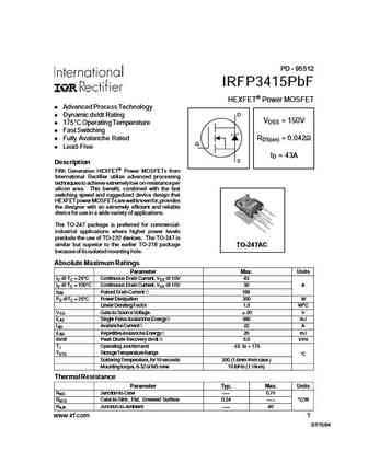
PD - 95512 IRFP3415PbF HEXFET Power MOSFET l Advanced Process Technology D l Dynamic dv/dt Rating VDSS = 150V l 175 C Operating Temperature l Fast Switching l Fully Avalanche Rated RDS(on) = 0.042 G l Lead-Free ID = 43A S Description Fifth Generation HEXFET Power MOSFETs from International Rectifier utilize advanced processing techniques to achieve extremely low on-resi... See More ⇒
irfp3415.pdf
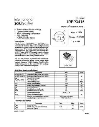
PD - 93962 IRFP3415 HEXFET Power MOSFET Advanced Process Technology D Dynamic dv/dt Rating VDSS = 150V 175 C Operating Temperature Fast Switching RDS(on) = 0.042 Fully Avalanche Rated G Description ID = 43A S Fifth Generation HEXFET Power MOSFETs from International Rectifier utilize advanced processing techniques to achieve extremely low on-resistance per silicon a... See More ⇒
irf5n3415.pdf
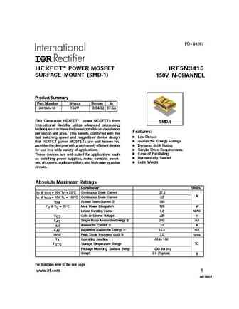
PD - 94267 HEXFET POWER MOSFET IRF5N3415 SURFACE MOUNT (SMD-1) 150V, N-CHANNEL Product Summary Part Number BVDSS RDS(on) ID 150V 0.042 37.5A IRF5N3415 Fifth Generation HEXFET power MOSFETs from SMD-1 International Rectifier utilize advanced processing techniques to achieve the lowest possible on-resistance Features per silicon unit area. This benefit, combined with the ... See More ⇒
2sk3415ls.pdf
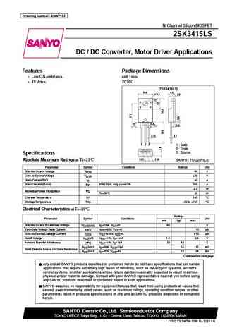
Ordering number ENN7153 2SK3415LS N-Channel Silicon MOSFET 2SK3415LS DC / DC Converter, Motor Driver Applications Features Package Dimensions Low ON-resistance. unit mm 4V drive. 2078C [2SK3415LS] 10.0 4.5 3.2 2.8 0.9 1.2 1.2 0.75 0.7 1 2 3 1 Gate 2 Drain 3 Source Specifications 2.55 2.55 Absolute Maximum Ratings at Ta=25 C SANYO TO-220FI(LS) Parameter... See More ⇒
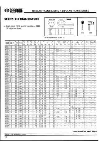
2n3415.pdf
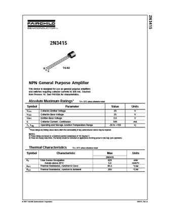
2N3415 B TO-92 C E NPN General Purpose Amplifier This device is designed for use as general purpose amplifiers and switches requiring collector currents to 300 mA. Sourced from Process 10. See PN100A for characteristics. Absolute Maximum Ratings* TA = 25 C unless otherwise noted Symbol Parameter Value Units V Collector-Emitter Voltage 25 V CEO V Collector-Base Voltage 25 V CBO V ... See More ⇒
2sc4061k 2sc3415s 2sc4015.pdf
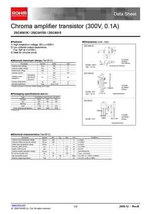
Chroma amplifier transistor (300V, 0.1A) 2SC4061K / 2SC3415S / 2SC4015 Features Dimensions (Unit mm) 1) High breakdown voltage. (BVCEO=300V) 2SC4061K 2) Low collector output capacitance. (Typ. 3pF at VCB=30V) 3) Ideal for chroma circuit. 1.6 2.8 (1) Emitter Absolute maximum ratings (Ta=25 C) (2) Base (3) Collector Parameter Symbol Limits Unit 0.3Min. ROHM ... See More ⇒
2sc3415s.pdf
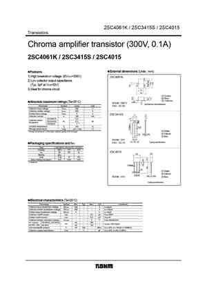
2SC4061K / 2SC3415S / 2SC4015 Transistors Chroma amplifier transistor (300V, 0.1A) 2SC4061K / 2SC3415S / 2SC4015 External dimensions (Units mm) Features 1) High breakdown voltage. (BVCEO=300V) 2SC4061K 2) Low collector output capacitance. (Typ. 3pF at VCB=30V) 3) Ideal for chroma circuit. 1.6 2.8 (1) Emitter (2) Base (3) Collector 0.3Min. Absolute maximum ratings (Ta=25 ... See More ⇒
2n3414 2n3415 2n3416 2n3417 mps3414 mps3415 mps3416 mps3417.pdf
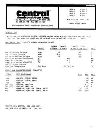
145 Adams Avenue, Hauppauge, NY 11788 USA Tel (631) 435-1110 Fax (631) 435-1824 ... See More ⇒
dmg3415u.pdf
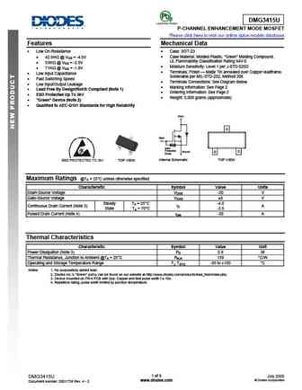
DMG3415U P-CHANNEL ENHANCEMENT MODE MOSFET Please click here to visit our online spice models database. Features Mechanical Data Low On-Resistance Case SOT-23 42.5m @ VGS = -4.5V Case Material Molded Plastic, Green Molding Compound. UL Flammability Classification Rating 94V-0 53m @ VGS = -2.5V Moisture Sensitivity Level 1 per J-STD-020D ... See More ⇒
dmg3415ufy4.pdf
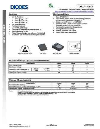
DMG3415UFY4 P-CHANNEL ENHANCEMENT MODE MOSFET Please click here to visit our online spice models database. Features Mechanical Data Low On-Resistance Case DFN2015H4-3 39m @ VGS = -4.5V Case Material Molded Plastic, Green Molding Compound. UL Flammability Classification Rating 94V-0 52m @ VGS = -2.5V Moisture Sensitivity Level 1 per J-STD-020 ... See More ⇒
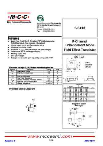
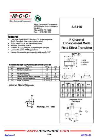
si3415a.pdf
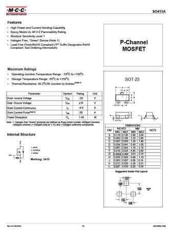
SI3415A Features High Power and Current Handing Capability Epoxy Meets UL 94 V-0 Flammability Rating Moisture Sensitivity Level 1 Halogen Free. Green Device (Note 1) P-Channel Lead Free Finish/RoHS Compliant ("P" Suffix Designates RoHS Compliant. See Ordering Information) MOSFET Maximum Ratings Operating Junction Temperature Range -55oC to +150oC ... See More ⇒
sil3415.pdf
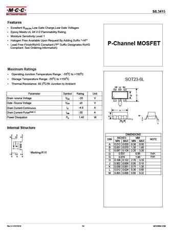
SIL3415 Features Excellent RDS(ON) Low Gate Charge,Low Gate Voltages Epoxy Meets UL 94 V-0 Flammability Rating Moisture Sensitivity Level 1 Halogen Free Available Upon Request By Adding Suffix "-HF" P-Channel MOSFET Lead Free Finish/RoHS Compliant ("P" Suffix Designates RoHS Compliant. See Ordering Information) Maximum Ratings Operating Junction Temperature Ran... See More ⇒
si3415b.pdf
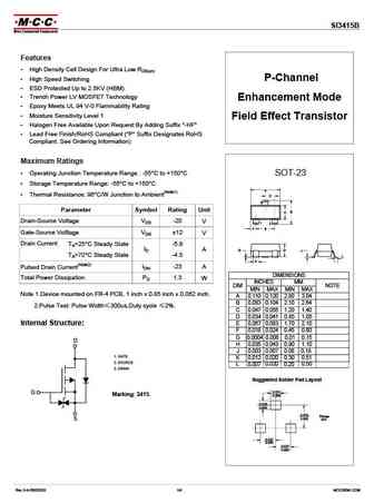
SI3415B Features High Density Cell Design For Ultra Low RDS(on) High Speed Switching P-Channel ESD Protected Up to 2.5KV (HBM) Trench Power LV MOSFET Technology Enhancement Mode Epoxy Meets UL 94 V-0 Flammability Rating Moisture Sensitivity Level 1 Field Effect Transistor Halogen Free Available Upon Request By Adding Suffix "-HF" Lead Free Finish/RoH... See More ⇒
2sc3415.pdf
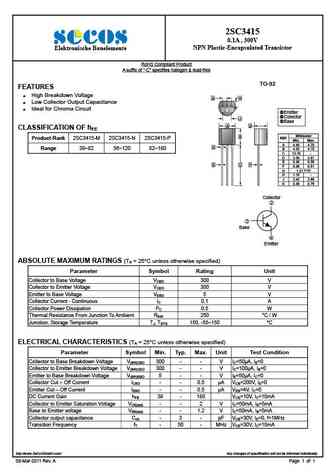
2SC3415 0.1A , 300V NPN Plastic-Encapsulated Transistor Elektronische Bauelemente RoHS Compliant Product A suffix of -C specifies halogen & lead-free TO-92 FEATURES High Breakdown Voltage G H Low Collector Output Capacitance Ideal for Chroma Circuit Emitter Collector J Base A D CLASSIFICATION OF hFE Millimeter B REF. Product-Rank 2SC... See More ⇒
cjk3415.pdf
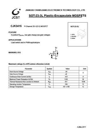
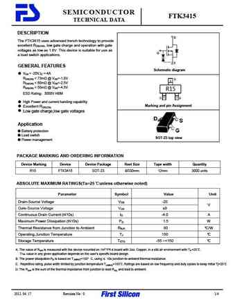
JIANGSU CHANGJIANG ELECTRONICS TECHNOLOGY CO., LTD SOT-23-3L Plastic-Encapsulate MOSFETS CJK3415 P-Channel 20-V(D-S) MOSFET SOT-23-3L FEATURE 1. GATE Excellent RDS(ON), low gate charge,low gate voltages 2. SOURCE 3. DRAIN APPLICATIONS Load switch and in PWM applicatopns D MARKING R15 G S Maximum ratings (Ta=25 unless otherwise noted) Parameter Symbol Value ... See More ⇒
cjl3415.pdf
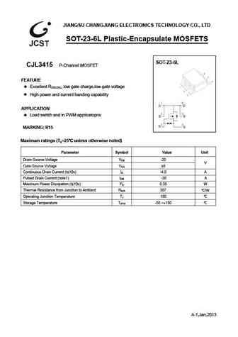
JIANGSU CHANGJIANG ELECTRONICS TECHNOLOGY CO., LTD SOT-23- L Plastic-Encapsulate MOSFETS SOT-23- CJ 3415 P-Channel MOSFET FEATURE Excellent RDS(ON), low gate charge,low gate voltage High power and current handing capability APPLICATION Load switch and in PWM applicatopns MARKING R15 Maximum ratings (Ta=25 unless otherwise noted) Parameter Symbol Value ... See More ⇒
cj3415.pdf
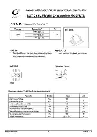
JIANGSU CHANGJIANG ELECTRONICS TECHNOLOGY CO., LTD SOT-23- L Plastic-Encapsulate MOSFETS CJ 3415 P-Channel 20V(D-S) MOSFET ID V(BR)DSS RDS(on)MAX SOT-23-6L 50m @-4.5V -4.0A -20V 60m @-2.5V 73m @-1. 8V FEATURE APPLICATION Excellent RDS(ON), low gate charge,low gate voltage Load switch and in PWM applicatopns High power and current handing capability MARKING Eq... See More ⇒
se3415.pdf
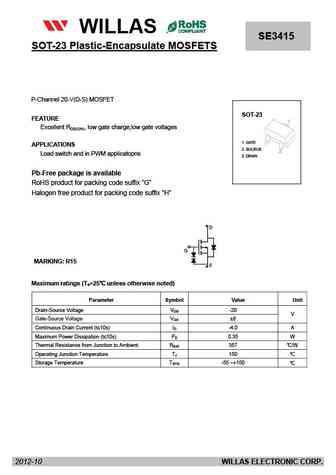
FM120-M WILLAS THRU SE3415 SOT-23 Plastic-Encapsulate MOSFETS FM1200-M 1.0A SURFACE MOUNT SCHOTTKY BARRIER RECTIFIERS -20V- 200V SOD-123 PACKAGE Pb Free Produ Package outline Features Batch process design, excellent power dissipation offers better reverse leakage current and thermal resistance. SOD-123H Low profile surface mounted application in order to optimize ... See More ⇒
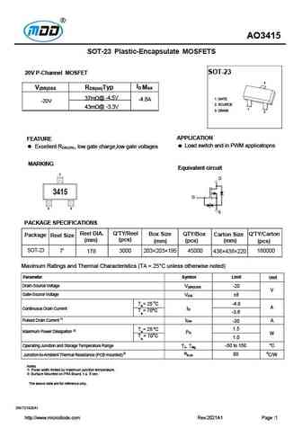
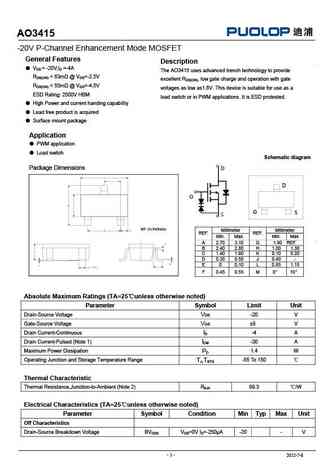
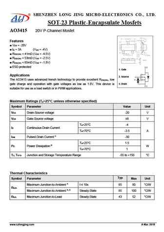
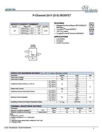
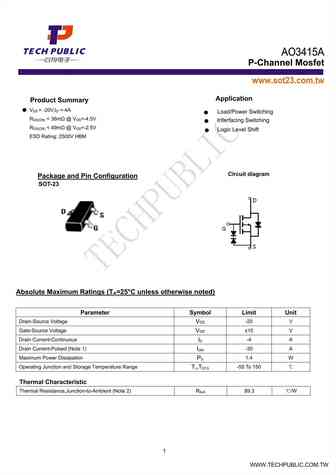
ao3415.pdf
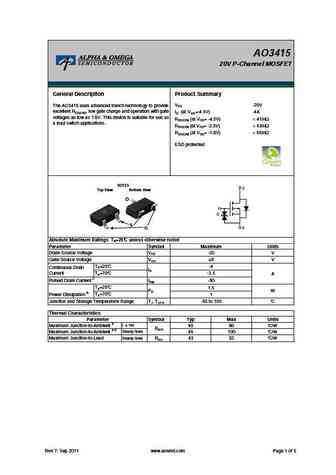
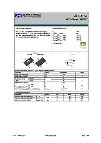
AO3415 20V P-Channel MOSFET General Description Product Summary VDS -20V The AO3415 uses advanced trench technology to provide excellent RDS(ON), low gate charge and operation with gate ID (at VGS=-4.5V) -4A voltages as low as 1.8V. This device is suitable for use as RDS(ON) (at VGS= -4.5V) ... See More ⇒
ao3415a.pdf
AO3415A 20V P-Channel MOSFET General Description Product Summary VDS -20V The AO3415A uses advanced trench technology to provide excellent RDS(ON), low gate charge and operation ID (at VGS=-4.5V) -5A with gate voltages as low as 1.8V. This device is suitable RDS(ON) (at VGS= -4.5V) ... See More ⇒
ao3415c.pdf
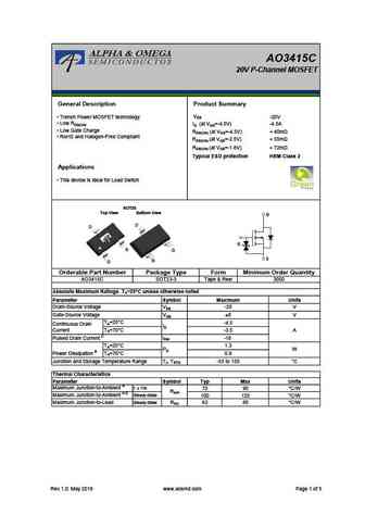
AO3415C 20V P-Channel MOSFET General Description Product Summary VDS Trench Power MOSFET technology -20V Low RDS(ON) ID (at VGS=-4.5V) -4.5A Low Gate Charge RDS(ON) (at VGS=-4.5V) ... See More ⇒
afp3415.pdf
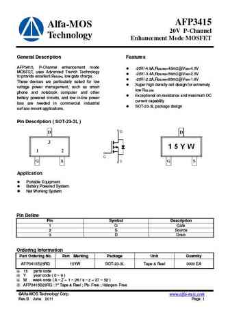
AFP3415 Alfa-MOS 20V P-Channel Technology Enhancement Mode MOSFET General Description Features AFP3415, P-Channel enhancement mode -20V/-4.9A,RDS(ON)=45m @VGS=4.5V MOSFET, uses Advanced Trench Technology -20V/-3.4A,RDS(ON)=58m @VGS=2.5V to provide excellent RDS(ON), low gate charge. -20V/-2.2A,RDS(ON)=85m @VGS=1.8V These devices are particularly suited for low ... See More ⇒
ao3415.pdf
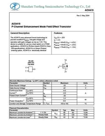
Shenzhen Tuofeng Semiconductor Technology Co., Ltd AO3415 Rev 3 May 2004 AO3415 P-Channel Enhancement Mode Field Effect Transistor General Description Features The AO3415 uses advanced trench technology to VDS (V) = -20V provide excellent RDS(ON), low gate charge and ID = -4 A operation with gate voltages as low as 1.8V. This RDS(ON) ... See More ⇒
btc3415a3.pdf
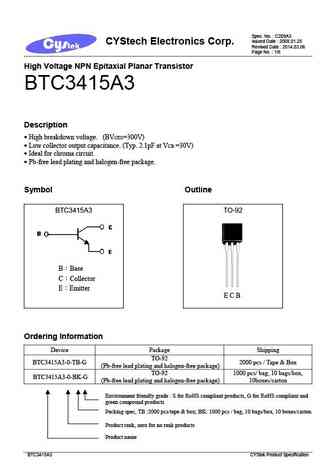
Spec. No. C209A3 Issued Date 2008.01.25 CYStech Electronics Corp. Revised Date 2014.03.06 Page No. 1/6 High Voltage NPN Epitaxial Planar Transistor BTC3415A3 Description High breakdown voltage. (BV =300V) CEO Low collector output capacitance. (Typ. 2.1pF at V =30V) CB Ideal for chroma circuit. Pb-free lead plating and halogen-free package. Symbo... See More ⇒
mtp3415kn3.pdf
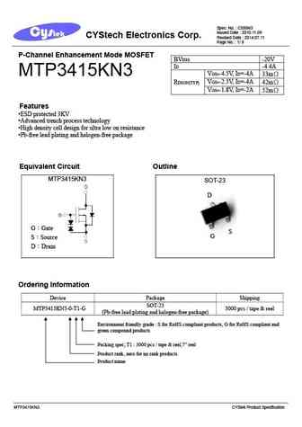
Spec. No. C589N3 Issued Date 2010.11.09 CYStech Electronics Corp. Revised Date 2014.07.11 Page No. 1/ 9 P-Channel Enhancement Mode MOSFET BVDSS -20V ID -4.4A VGS=-4.5V, ID=-4A MTP3415KN3 33m VGS=-2.5V, ID=-4A 42m RDSON(TYP) VGS=-1.8V, ID=-2A 52m Features ESD protected 3KV Advanced trench process technology High density cell design for ultra lo... See More ⇒
3415a.pdf
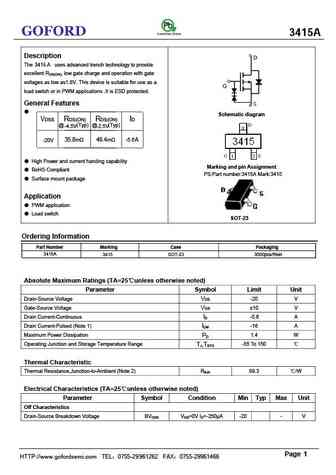
GOFORD 3415A Description The 3415 A uses advanced trench technology to provide excellent RDS(ON), low gate charge and operation with gate voltages as low as1.8V. This device is suitable for use as a load switch or in PWM applications .It is ESD protected. General Features Schematic diagram VDSS RDS(ON) RDS(ON) ID (Typ) @ (Typ) @-2.5V -4.5V 35.8m 46.4m -5.6 -20... See More ⇒
sts3415.pdf
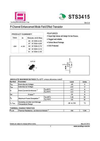
Gr P Pr P P STS3415 a S mHop Microelectronics C orp. Ver 2.0 P-Channel Enhancement Mode Field Effect Transistor FEATURES PRODUCT SUMMARY Super high dense cell design for low RDS(ON). VDSS ID RDS(ON) (m ) Max Rugged and reliable. 46 @ VGS=-4.5V Suface Mount Package. 47 @ VGS=-4.0V ESD Protected. 49 @ VGS=-3.7V -20V -4.2A 54 @ VGS=-3.1V 61 @ VGS=-2.5V D SOT-23 G D S G... See More ⇒
brcs3415mc.pdf
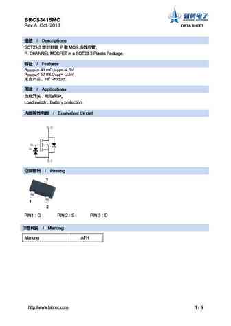
BRCS3415MC Rev.A .Oct.-2018 DATA SHEET / Descriptions SOT23-3 P MOS P- CHANNEL MOSFET in a SOT23-3 Plastic Package. / Features RDS(ON)... See More ⇒
lp3415elt1g s-lp3415elt1g.pdf
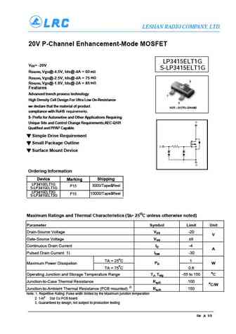
LESHAN RADIO COMPANY, LTD. 20V P-Channel Enhancement-Mode MOSFET LP3415ELT1G V = -20V DS S-LP3415ELT1G R Vgs@-4.5V, Ids@-4A = 60 m DS(ON), m R DS(ON), Vgs@-2.5V, Ids@-4A = 75 3 m RDS(ON), Vgs@-1.8V, Ids@-2A = 85 Features Advanced trench process technology 1 High Density Cell Design For Ultra Low On-Resistance 2 we declare that the material of product SOT 23 (... See More ⇒
dmg3415u.pdf
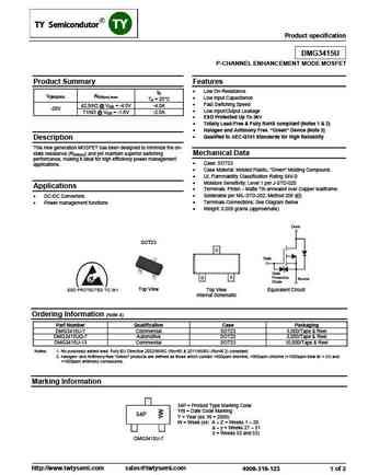
Product specification DMG3415U P-CHANNEL ENHANCEMENT MODE MOSFET Product Summary Features Low On-Resistance ID V(BR)DSS RDS(on) max Low Input Capacitance TA = 25 C Fast Switching Speed 42.5m @ VGS = -4.5V -4.0A -20V Low Input/Output Leakage 71m @ VGS = -1.8V -2.0A ESD Protected Up To 3kV Totally Lead-Free & Fully RoHS compliant (Notes 1 & ... See More ⇒
ftk3415l.pdf
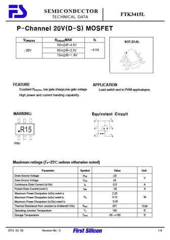
SEMICONDUCTOR FTK3415L TECHNICAL DATA P-Channel 20V(D-S) MOSFET ID V(BR)DSS RDS(on)MAX SOT-23-6L 50m @-4.5V -4.0A -20V 60m @-2.5V 73m @-1. 8V FEATURE APPLICATION Excellent RDS(ON), low gate charge,low gate voltage Load switch and in PWM applicatopns High power and current handing capability MARKING Equivalent Circuit PIN1 Maximum ratings (Ta=25 unless otherwise ... See More ⇒
ftk3415.pdf
SEMICONDUCTOR FTK3415 TECHNICAL DATA DESCRIPTION D The FTK3415 uses advanced trench technology to provide excellent RDS(ON), low gate charge and operation with gate voltages as low as 1.8V. This device is suitable for use as G a load switch applications. S GENERAL FEATURES Schematic diagram VDS = -20V,ID =-4A RDS(ON) ... See More ⇒
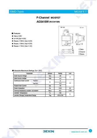
ao3415.pdf
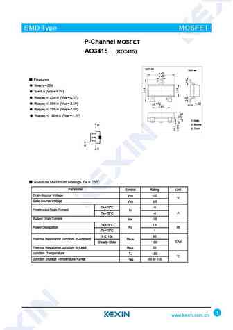
SMD Type MOSFET P-Channel MOSFET AO3415 (KO3415) SOT-23 Unit mm +0.1 2.9-0.1 +0.1 0.4 -0.1 Features 3 VDS (V) =-20V ID =-5 A (VGS =-4.5V) RDS(ON) 43m (VGS =-4.5V) 1 2 +0.1 0.95-0.1 0.1+0.05 RDS(ON) 55m (VGS =-2.5V) -0.01 +0.1 1.9-0.1 RDS(ON) 75m (VGS =-1.8V) RDS(ON) 100m (VGS =-1.5V) 1. Gate 2. Source D 3. Drain... See More ⇒
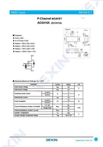
ao3415a.pdf
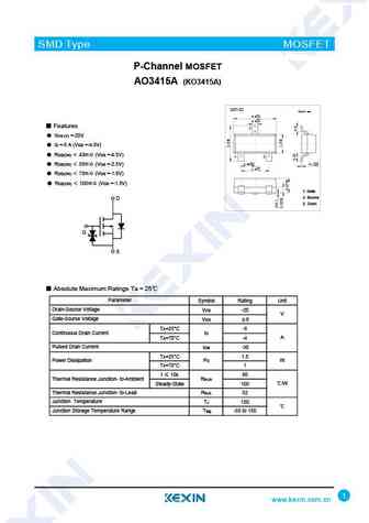
SMD Type MOSFET P-Channel MOSFET AO3415A (KO3415A) SOT-23 Unit mm +0.1 2.9-0.1 +0.1 0.4 -0.1 Features 3 VDS (V) =-20V ID =-5 A (VGS =-4.5V) RDS(ON) 43m (VGS =-4.5V) 1 2 +0.1 0.95-0.1 0.1+0.05 RDS(ON) 55m (VGS =-2.5V) -0.01 +0.1 1.9-0.1 RDS(ON) 75m (VGS =-1.8V) RDS(ON) 100m (VGS =-1.5V) 1. Gate 2. Source D 3. Dra... See More ⇒
ko3415a.pdf
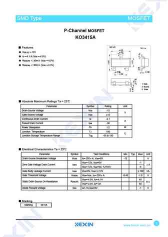
SMD Type MOSFET Transistors P-Channel MOSFET KO3415A SOT-23 Features Unit mm +0.1 2.9 -0.1 +0.1 VDS (V) =-12V 0.4-0.1 3 ID =-4.1 A (VGS =-4.5V) RDS(ON) 45m (VGS =-4.5V) RDS(ON) 60m (VGS =-2.5V) 1 2 +0.1 +0.05 0.95 -0.1 0.1 -0.01 +0.1 1.9 -0.1 1. Gate 2. Source 3. Drain Absolute Maximum Ratings Ta = 25 Parameter Symbol Rating U... See More ⇒
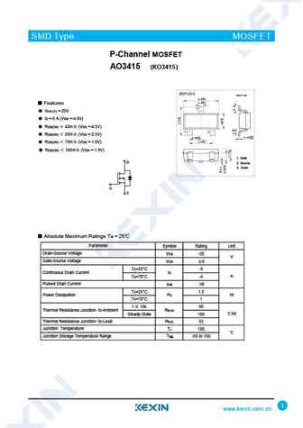
ao3415w.pdf
SMD Type MOSFET P-Channel MOSFET (KO3415W) AO3415W Features VDS (V) =-20V ID =-4A (VGS =-4.5V) RDS(ON) 50m (VGS =-4.5V) RDS(ON) 60m (VGS =-2.5V) RDS(ON) 75m (VGS =-1.8V) 1 Gate 2 Source 3 Drain Absolute Maximum Ratings Ta = 25 Parameter Symbol Rating Unit Drain-Source Voltage VDS -20 V Gate-Source Voltage VGS 8 Conti... See More ⇒
ao3415 ko3415.pdf
SMD Type MOSFET P-Channel MOSFET AO3415 (KO3415) SOT-23-3 Unit mm +0.2 2.9-0.1 +0.1 0.4 -0.1 Features 3 VDS (V) =-20V ID =-5 A (VGS =-4.5V) RDS(ON) 43m (VGS =-4.5V) 1 2 RDS(ON) 55m (VGS =-2.5V) +0.02 +0.1 0.15 -0.02 0.95 -0.1 +0.1 1.9-0.2 RDS(ON) 75m (VGS =-1.8V) RDS(ON) 100m (VGS =-1.5V) 1. Gate D 2. Source 3... See More ⇒
ao3415as.pdf
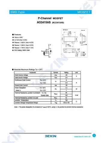
SMD Type MOSFET P-Channel MOSFET AO3415AS (KO3415AS) SOT-23-3 Unit mm +0.2 2.9 -0.1 +0.1 0.4-0.1 Features 3 VDS (V) =-20V ID =-4A (VGS =-4.5V) RDS(ON) 45m (VGS =-4.5V) 1 2 +0.02 +0.1 0.15 -0.02 0.95 -0.1 D RDS(ON) 54m (VGS =-2.5V) +0.1 1.9 -0.2 RDS(ON) 75m (VGS =-1.8V) ESD Rating 3000V HBM G 1. Gate 2. Source 3. Dra... See More ⇒
ao3415-3.pdf

SMD Type MOSFET P-Channel MOSFET AO3415 (KO3415) SOT-23-3 Unit mm +0.2 2.9-0.1 +0.1 0.4 -0.1 Features 3 VDS (V) =-20V ID =-5 A (VGS =-4.5V) RDS(ON) 43m (VGS =-4.5V) 1 2 RDS(ON) 55m (VGS =-2.5V) +0.02 +0.1 0.15 -0.02 0.95 -0.1 +0.1 1.9-0.2 RDS(ON) 75m (VGS =-1.8V) RDS(ON) 100m (VGS =-1.5V) 1. Gate D 2. Source 3... See More ⇒
ao3415a-3.pdf
SMD Type MOSFET P-Channel MOSFET AO3415A (KO3415A) SOT-23-3 Unit mm +0.2 2.9 -0.1 +0.1 0.4 -0.1 3 Features VDS (V) =-20V ID =-5 A (VGS =-4.5V) 1 2 RDS(ON) 43m (VGS =-4.5V) +0.02 +0.1 0.15 -0.02 0.95 -0.1 +0.1 1.9 -0.2 RDS(ON) 55m (VGS =-2.5V) RDS(ON) 75m (VGS =-1.8V) RDS(ON) 100m (VGS =-1.5V) 1. Gate 2. Source ... See More ⇒
pja3415ae.pdf
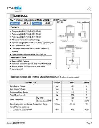
PPJA3415AE 20V P-Channel Enhancement Mode MOSFET ESD Protected SOT-23 Unit inch(mm) Voltage -20 V Current -4.3A Features RDS(ON) , VGS@-4.5V, ID@-4.3A... See More ⇒
pja3415.pdf
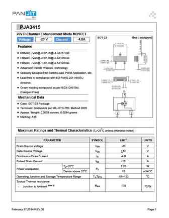
PPJA3415 20V P-Channel Enhancement Mode MOSFET SOT-23 Unit inch(mm) Voltage -20 V Current -4.0A Features RDS(ON) , VGS@-4.5V, ID@-4.0A... See More ⇒
am3415a.pdf
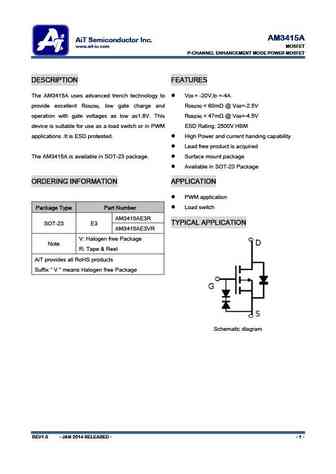
AM3415A AiT Semiconductor Inc. www.ait-ic.com MOSFET P-CHANNEL ENHANCEMENT MODE POWER MOSFET DESCRIPTION FEATURES The AM3415A uses advanced trench technology to V = -20V,I =-4A DS D provide excellent R , low gate charge and R ... See More ⇒
am3415.pdf
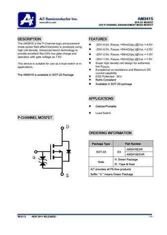
AiT Semiconductor Inc. AM3415 www.ait-ic.com SOT-23 MOSFET -20V P-CHANNEL ENHANCEMENT MODE MOSFET DESCRIPTION FEATURES The AM3415 is the P-Channel logic enhancement -20V/-4.0A, R =45m (typ.)@V =-4.5V DS(ON) GS mode power field effect transistor is produced using -20V/-4.0A, R =54m (typ.)@V =-2.5V DS(ON) GS high cell density. Advanced trench technology to provide ex... See More ⇒
blm3415.pdf
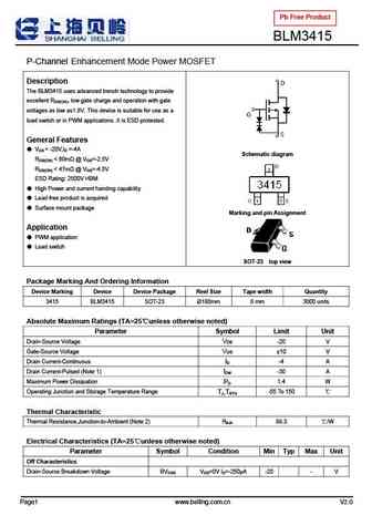
Pb Free Product BLM3415 P-Channel Enhancement Mode Power MOSFET Description The BLM3415 uses advanced trench technology to provide excellent RDS(ON), low gate charge and operation with gate voltages as low as1.8V. This device is suitable for use as a load switch or in PWM applications .It is ESD protested. General Features VDS = -20V,ID =-4A Schematic diagram RDS(ON) ... See More ⇒
elm33415ca.pdf
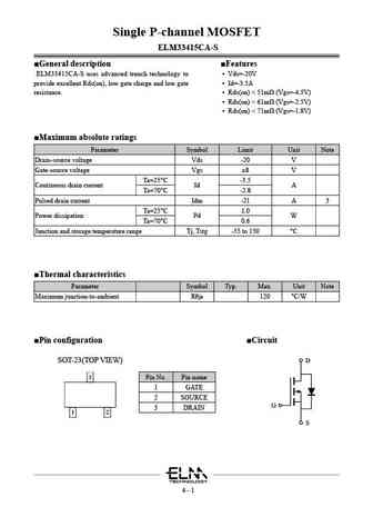
Single P-channel MOSFET ELM33415CA-S General description Features ELM33415CA-S uses advanced trench technology to Vds=-20V provide excellent Rds(on), low gate charge and low gate Id=-3.5A resistance. Rds(on) ... See More ⇒
elm13415ca.pdf
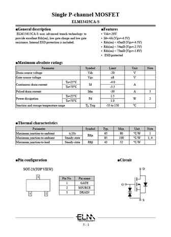
Single P-channel MOSFET ELM13415CA-S General description Features ELM13415CA-S uses advanced trench technology to Vds=-20V provide excellent Rds(on), low gate charge and low gate Id=-4A (Vgs=-4.5V) resistance. Internal ESD protection is included. Rds(on) ... See More ⇒
gsm3415.pdf
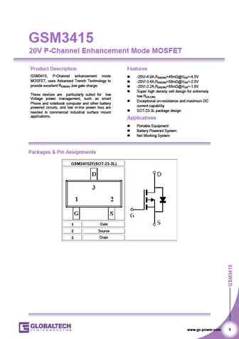
GSM3415 20V P-Channel Enhancement Mode MOSFET Product Description Features GSM3415, P-Channel enhancement mode -20V/-4.9A,RDS(ON)=45m @VGS=-4.5V MOSFET, uses Advanced Trench Technology to -20V/-3.4A,RDS(ON)=58m @VGS=-2.5V provide excellent RDS(ON) ,low gate charge. -20V/-2.2A,RDS(ON)=85m @VGS=-1.8V Super high density cell design for extremely These devic... See More ⇒
kia3415.pdf
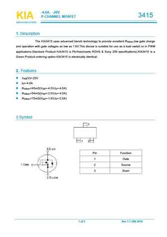
-4.0A -20V 3415 P-CHANNELMOSFET KIA KIA KIA SEMICONDUCTORS SEMICONDUCTORS SEMICONDUCTORS 1.Description The KIA3415 uses advanced trench technology to provide excellent R ,lowgate charge DS(on) and operation with gate voltages as lowas 1.8V.This device is suitable for use as a load switch or in PWM applications.Standard Product KIA3415 is Pb-free(meets ROHS & Sony 259 specificatio... See More ⇒
mmp3415e.pdf
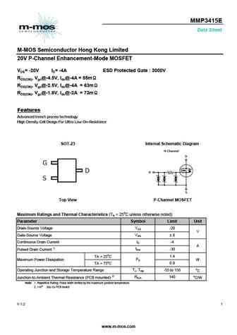
MMP3415E Data Sheet M-MOS Semiconductor Hong Kong Limited 20V P-Channel Enhancement-Mode MOSFET VDS= -20V ID= -4A ESD Protected Gate 3000V RDS(ON), Vgs@-4.5V, Ids@-4A = 55m RDS(ON), Vgs@-2.5V, Ids@-4A = 63m RDS(ON), Vgs@-1.8V, Ids@-2A = 73m Features Advanced trench process technology High Density Cell Design For Ultra Low On-Resistance SOT-23 Internal Schematic Diagram To... See More ⇒
nce3415y.pdf
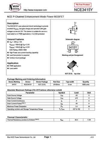
Pb Free Product http //www.ncepower.com NCE3415Y NCE P-Channel Enhancement Mode Power MOSFET Description The NCE3415Y uses advanced trench technology to provide excellent RDS(ON), low gate charge and operation with gate voltages as low as1.8V. This device is suitable for use as a load switch or in PWM applications .It is ESD protested. Schematic diagram General Features ... See More ⇒
nce3415.pdf
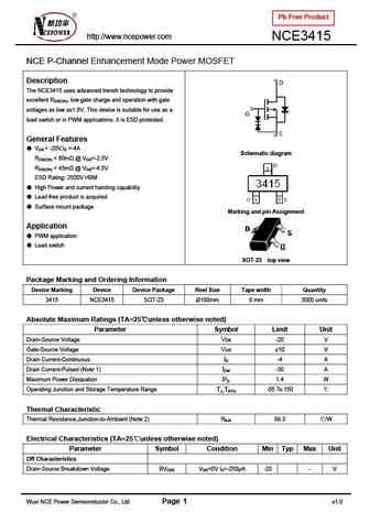
Pb Free Product http //www.ncepower.com NCE3415 NCE P-Channel Enhancement Mode Power MOSFET Description The NCE3415 uses advanced trench technology to provide excellent RDS(ON), low gate charge and operation with gate voltages as low as1.8V. This device is suitable for use as a load switch or in PWM applications .It is ESD protested. General Features VDS = -20V,ID =-4A S... See More ⇒
nce3415e.pdf
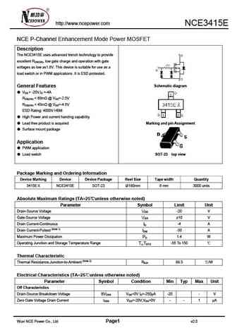
http //www.ncepower.com NCE3415E NCE P-Channel Enhancement Mode Power MOSFET Description The NCE3415E uses advanced trench technology to provide excellent RDS(ON), low gate charge and operation with gate voltages as low as1.8V. This device is suitable for use as a load switch or in PWM applications .It is ESD protested. Schematic diagram General Features VDS = -20V,ID =-4... See More ⇒
smc3415a.pdf
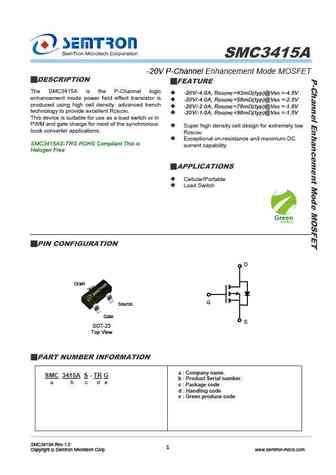
SMC3415A -20V P-Channel Enhancement Mode MOSFET DESCRIPTION FEATURE The SMC3415A is the P-Channel logic -20V/-4.0A, RDS(ON) =43m (typ)@VGS =-4.5V enhancement mode power field effect transistor is -20V/-4.0A, RDS(ON) =58m (typ)@VGS =-2.5V produced using high cell density. advanced trench -20V/-2.0A, RDS(ON) =78m (typ)@VGS =-1.8V technology to provide excel... See More ⇒
sl3415.pdf
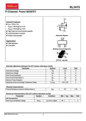
SL3415 P-Channel Power MOSFET General Features VDS = -20V,ID =-4A RDS(ON) ... See More ⇒
ao3415a.pdf
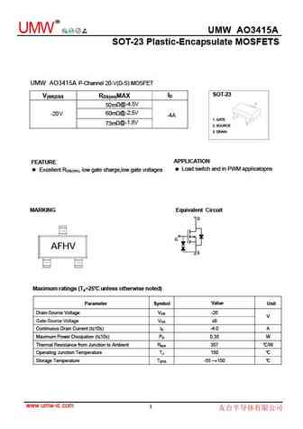
R UMW UMW AO3415A SOT-23 Plastic-Encapsulate MOSFETS UMW AO3415A P-Channel 20-V(D-S) MOSFET SOT-23 ID V(BR)DSS RDS(on)MAX 50m @-4.5V -20V 60m @-2.5V -4A 1. GATE 73m @-1.8V 2. SOURCE 3. DRAIN APPLICATION FEATURE Load switch and in PWM applicatopns Excellent RDS(ON), low gate charge,low gate voltages MARKING Equivalent Circuit D G AFHV S Maximum ratings... See More ⇒
atm3415kpsa.pdf
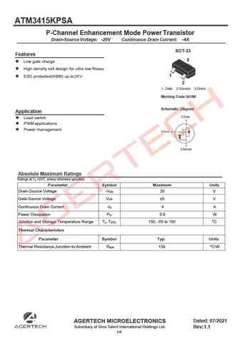
ATM3415KPSA P-Channel Enhancement Mode Power Transistor Drain-Source Voltage -20V Continuous Drain Current -4A Features Low gate charge High density cell design for ultra low R DS(on) ESD protected(HBM) up to2KV Application Load switch PWMapplications Power management Absolute Maximum Ratings Ratings at T =25 unless otherwise specified. A Parameter Sy... See More ⇒
as3415e.pdf
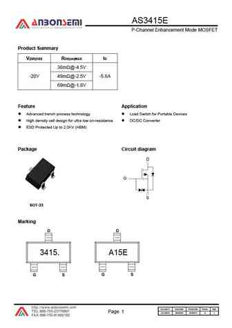
AS3415E P-Channel Enhancement Mode MOSFET Product Summary V R I (BR)DSS DS(on)MAX D 36m @-4.5V -20V 49m @-2.5V -5.6A 69m @-1.8V Feature Application Advanced trench process technology Load Switch for Portable Devices High density cell design for ultra low on-resistance DC/DC Converter ESD Protected Up to 2.0KV (HBM) Package Circuit diagram SOT-23 ... See More ⇒
bm3415e.pdf
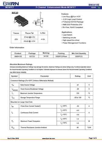
BM3415E MOSFET ROHS P-Channel Enhancement-Mode MOSFET SOT-23 - Features Low RDS(on) @VGS=-4.5V -3.3V Logic Level Control P Channel SOT23 Package HMB ESD Protection 2KV Pb-Free, RoHS Compliant Applications V R Typ I Max (BR)DSS DS(ON) D Load Switch 37m @-4.5V Switching circuits -20V -4.8A High-speed line driver 43m @ -3.3V Power Manage... See More ⇒
fs3415k.pdf
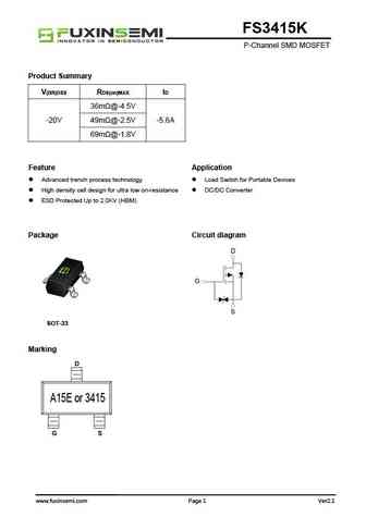
FS3415K P-Channel SMD MOSFET Product Summary V R I (BR)DSS DS(on)MAX D 36m @-4.5V -20V 49m @-2.5V -5.6A 69m @-1.8V Feature Application Advanced trench process technology Load Switch for Portable Devices High density cell design for ultra low on-resistance DC/DC Converter ESD Protected Up to 2.0KV (HBM) Package Circuit diagram SOT-23 Marking A15E... See More ⇒
ev3415.pdf
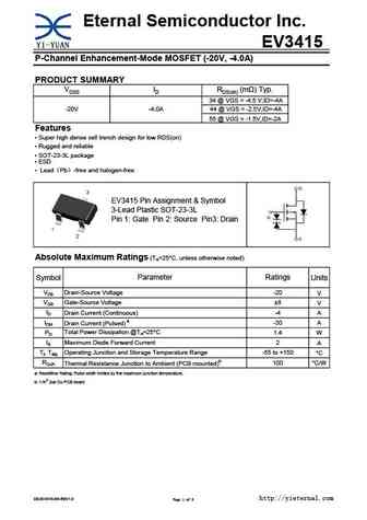
Eternal Semiconductor Inc. EV3415 P-Channel Enhancement-Mode MOSFET (-20V, -4.0A) PRODUCT SUMMARY VDSS ID RDS(on) (m ) Typ. 34 @ VGS = -4.5 V,ID=-4A -20V -4.0A 44 @ VGS = -2.5V,ID=-4A 55 @ VGS = -1.5V,ID=-2A Features Super high dense cell trench design for low RDS(on) Rugged and reliable SOT-23-3L package ESD Lead Pb -free and halogen-free EV3415 Pin Ass... See More ⇒
ao3415.pdf
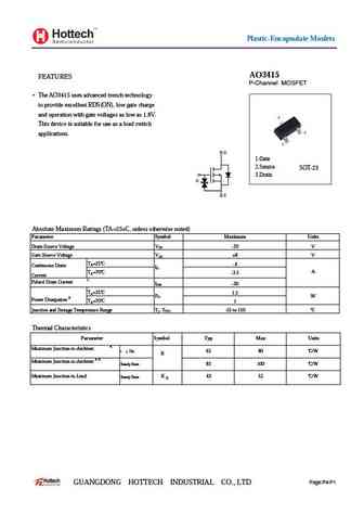
Plastic-Encapsulate Mosfets AO3415 FEATURES P-Channel MOSFET The AO3415 uses advanced trench technology to provide excellent RDS(ON), low gate charge and operation with gate voltages as low as 1.8V. This device is suitable for use as a load switch applications. D 1.Gate 2.Source SOT-23 3.Drain G S Absolute Maximum Ratings (TA=25oC, unless otherwise noted) Parameter Symbol Maxim... See More ⇒
ao3415.pdf
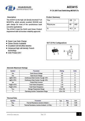
AO3415 P-Ch 20V Fast Switching MOSFETs Description Product Summary The AO3415 is the high cell density trenched P-ch VDS -20 V MOSFETs, which provide excellent RDSON and gate charge for most of the synchronous buck RDS(ON),max 45 m converter applications. ID -4.3 A The AO3415 meet the RoHS and Green Product requirement with full function reliability approved. Super L... See More ⇒
hsw3415.pdf
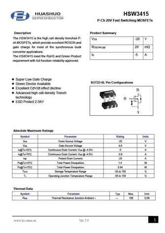
HSW3415 P-Ch 20V Fast Switching MOSFETs Description Product Summary The HSW3415 is the high cell density trenched P- VDS -20 V ch MOSFETs, which provide excellent RDSON and gate charge for most of the synchronous buck RDS(ON),typ 29 m converter applications. ID -5 A The HSW3415 meet the RoHS and Green Product requirement with full function reliability approved. Super ... See More ⇒
hss3415e.pdf
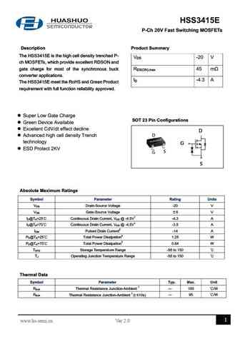
HSS3415E P-Ch 20V Fast Switching MOSFETs Description Product Summary The HSS3415E is the high cell density trenched P- VDS -20 V ch MOSFETs, which provide excellent RDSON and gate charge for most of the synchronous buck RDS(ON),max 45 m converter applications. ID -4.3 A The HSS3415E meet the RoHS and Green Product requirement with full function reliability approved. l Sup... See More ⇒
hx3415.pdf
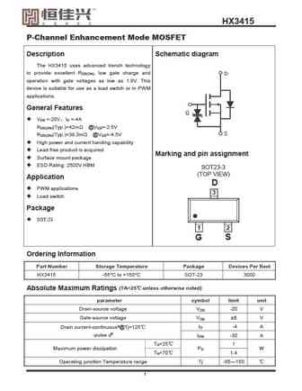
HX3415 P-Channel Enhancement Mode MOSFET Description Schematic diagram The HX3415 uses advanced trench technology to provide excellent R , low gate charge and DS(ON) operation with gate voltages as low as 1.8V. This device is suitable for use as a load switch or in PWM applications. General Features V =-20V I =-4A DS D R (Typ.)=42m @V =-2.5V DS(ON) GS R (Typ.)=38.3m @V... See More ⇒
hx3415a.pdf
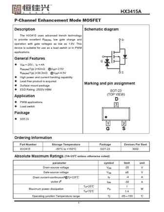
HX3415A P-Channel Enhancement Mode MOSFET Description Schematic diagram The HX3415 uses advanced trench technology to provide excellent R , low gate charge and DS(ON) operation with gate voltages as low as 1.8V. This device is suitable for use as a load switch or in PWM applications. General Features V =-20V I =-4A DS D R (Typ.)=42m @V =-2.5V DS(ON) GS R (Typ.)=38.3m @... See More ⇒
2n3403 2n3404 2n3405 2n3414 2n3415 2n3416 2n3417 2n3702 2n3703 2n3704 2n3705 2n3706 2n3707 2n3708 2n3709 2n3710.pdf
... See More ⇒
jmtl3415kl.pdf
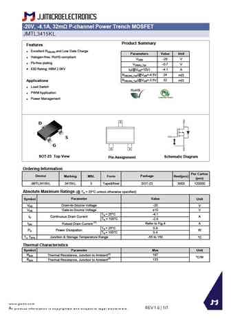
-20V, -4.1A, 32m P-channel Power Trench MOSFET JMTL3415KL Product Summary Features Excellent RDS(ON) and Low Gate Charge Parameters Value Unit Halogen-free; RoHS-compliant VDSS -20 V Pb-free plating VGS(th)_Typ -0.7 V ESD Rating HBM 2.0KV ID(@VGS=10V) -4.1 A RDS(ON)_Typ(@VGS=-4.5V 24 mW RDS(ON)_Typ(@VGS=-2.5V 32 mW Applications Load Switch PWM Applicat... See More ⇒
jmtj3415kl.pdf
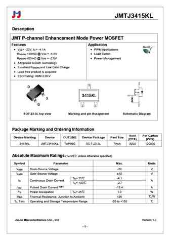
JMTJ3415KL Description JMT P-channel Enhancement Mode Power MOSFET Features Application V = -20V, I = -4.1A PWM Applications DS D R ... See More ⇒
jmtl3415k.pdf
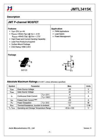
JMTL3415K Description JMT P-channel MOSFET Features Application V =-20V, I =-4A PWM Applications DS D R =38m (Typ.) @ VGS = -4.5V Load Switch DS(ON) R =48m (Typ.) @ VGS = -2.5V Power Management DS(ON) High Power and Current Handing Capability Lead Free Product is Acquired Surface Mount Package ESD Rating HBM 2.0KV Package ... See More ⇒
jmtm3415kl.pdf
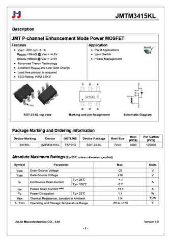
JMTM3415KL Description JMT P-channel Enhancement Mode Power MOSFET Features Application V = -20V, I = -4.1A PWM Applications DS D R ... See More ⇒
jst3415c.pdf
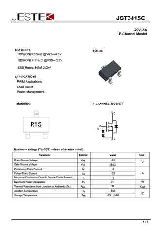
JST3415C -20V,-5A P-Channel Mosfet FEATURES SOT-23 RDS(ON) 32m @VGS=-4.5V RDS(ON) 51m @VGS=-2.5V ESD Rating HBM 2.0KV APPLICATIONS PWM Applications Load Switch Power Management MARKING P-CHANNEL MOSFET Maximum ratings (TC=25 unless otherwise noted) Parameter Symbol Value Unit Drain-Source Voltage VDS -20 V Gate-Source Voltage V 12 GS I -5 D Continuous Drai... See More ⇒
ao3415.pdf
AO3415 SOT-23 Plastic-Encapsulate MOSFETS SOT-23 20V P-Channel MOSFET 3 ID Max V(BR)DSS RDS(on)Typ 37m @ -4.5V 1. GATE -4.8A -20V 2. SOURCE 43m @ -3.3V 1 3. DRAIN 2 APPLICATION FEATURE Load switch and in PWM applicatopns Excellent RDS(ON), low gate charge,low gate voltages MARKING Equivalent circuit D 3415 G S PACKAGE SPECIFICATIONS Reel DI... See More ⇒
ao3415ai-ms.pdf
www.msksemi.com AO3415AI-MS Semiconductor Compiance D VDS -20V I (at V =-4.5V) -4A D GS R (at V = -4.5V) ... See More ⇒
pjm3415psa.pdf
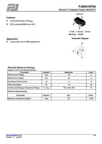
PJM3415PSA Silicon P-Channel Power MOSFET SOT-23 Features Low Gate Charge and RDS(on) ESD protected(HBM) up to 2KV 1. Gate 2.Source 3.Drain Marking 3415K Schematic Diagram Application Load switch and in PWM applications D G S Absolute Maximum Ratings Ratings at TA =25 unless otherwise specified. Parameter Symbol Maximum Units Drain-Source Voltage -V 20 V DS ... See More ⇒
3415e.pdf
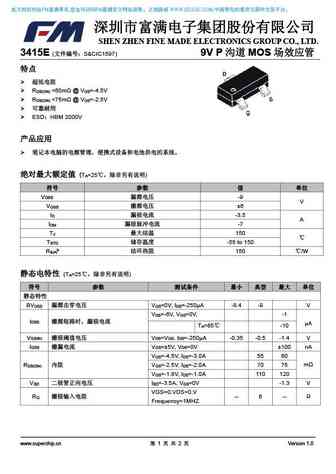
FM , FM WWW.SZLCSC.COM, SHEN ZHEN FINE MADE ELECTRONICS GROUP CO., LTD. 3415E ( S&CIC1597) 9V P MOS R ... See More ⇒
ao3415.pdf
AO3415 -20V P-Channel Enhancement Mode MOSFET General Features Description VDS = -20V,ID =-4A The AO3415 uses advanced trench technology to provide RDS(ON) ... See More ⇒
agm3415e.pdf
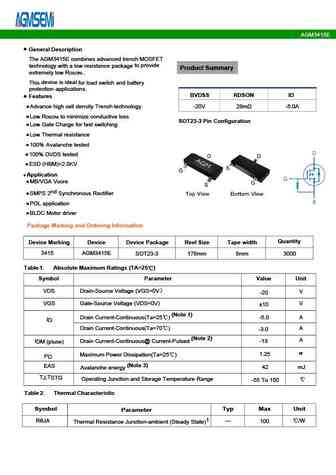
AGM3415E Typical Performance Characteristics Figure 2 Typical Transfer Characteristics Figure1 Output Characteristics -I (A) D -I (A) D 20 20 16 16 VGS=- 100 4.5V 12 12 VGS=-3V 25 -2V 8 8 4 4 -1.5V -V (V) GS -V (V) DS 0 0 0 1 2 3 4 5 0 0.3 0.6 0.9 1.2 1.5 1.8 2.1 2.4 2.7 Figure 3 On-resistance vs. Drain Current Figure 4 Body Diode Characteristics I (A... See More ⇒
a03415.pdf
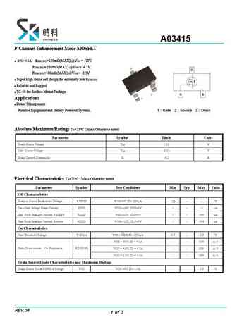
A03415 P-Channel Enhancement Mode MOSFET -25V/-4.2A, RDS(ON) =130m (MAX) @VGS = -10V. RDS(ON) = 150m (MAX) @VGS = -4.5V. RDS(ON) =180m (MAX) @VGS = -2.5V. Super High dense cell design for extremely low RDS(ON) Reliable and Rugged SC-59 for Surface Mount Package Applications Power Management Portable Equipment and Battery Powered Systems. 1 Gate 2 Source ... See More ⇒
wtm3415.pdf
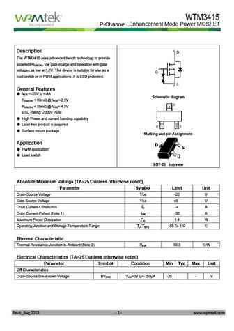
WTM3415 Enhancement Mode Power MOSFET P-Channel Description The WTM3415 uses advanced trench technology to provide excellent RDS(ON), low gate charge and operation with gate voltages as low as1.8V. This device is suitable for use as a load switch or in PWM applications .It is ESD protested. General Features VDS = -20V,ID =-4A Schematic diagram RDS(ON) ... See More ⇒
ao3415.pdf
SHENZHEN LONG JING MICRO-ELECTRONICS CO., LTD. SOT-23 Plastic-Encapsulate Mosfets AO3415 20V P-Channel Mosfet Features V = -20V DS I = 3A (V = -4V) D GS R ... See More ⇒
tf3415.pdf
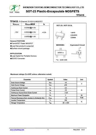
SHENZHEN TUOFENG SEMICONDUCTOR TECHNOLOGY CO.,LTD SOT-23 Plastic-Encapsulate MOSFETS TF3415 P-Channel 15-V(D-S) MOSFET TF3415 V(BR)DSS RDS(on)MAX ID SOT-23 SOT-23-3L / 0.039 @-4.5V 3 -15V 0.052 @-2.5V -4.3A 1.GATE 2.SOURCE 0.063 @-1.8V 3.DRAIN 1 2 General FEATURE TrenchFET Power MOSFET MARKING Equivalent Circuit Lead free product is acquired Surface mount packa... See More ⇒
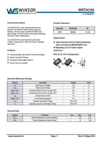
wst3415.pdf

WST3415 P-Ch MOSFET General Description Product Summery The WST3415 is the highest performance trench BVDSS RDSON ID P-ch MOSFET with extreme high cell density , which provide excellent RDSON and gate charge -20V 44m -5.5A for most of the small power switching and load switch applications. Applications The WST3415 meet the RoHS and Green Product requirement , with full ... See More ⇒
wst3415a.pdf
WST3415A P-Ch MOSFET General Description Product Summery The WST3415A is the highest performance BVDSS RDSON ID trench P-ch MOSFET with extreme high cell density , which provide excellent RDSON and -20V 58m -5.3A gate charge for most of the small power switching and load switch applications. Applications The WST3415A meet the RoHS and Green Product requirement , with fu... See More ⇒
sts3415.pdf
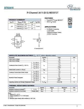
STS3415 www.VBsemi.tw P-Channel 30 V (D-S) MOSFET FEATURES PRODUCT SUMMARY TrenchFET Power MOSFET 100 % Rg Tested VDS (V) RDS(on) ( ) Typ. ID (A)a Qg (Typ.) 0.046 at VGS = - 10 V - 5.6 0.049 at VGS = - 6 V - 5 11.4 nC - 30 APPLICATIONS 0.054 at VGS = - 4.5 V -4.5 For Mobile Computing - Load Switch - Notebook Adaptor Switch S TO-236 - DC/DC Converter (SOT-23)... See More ⇒
yjq3415a.pdf
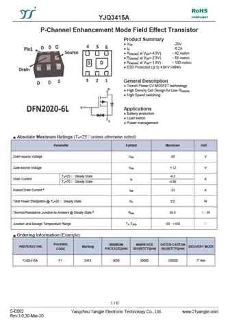
RoHS COMPLIANT YJQ3415A P-Channel Enhancement Mode Field Effect Transistor Product Summary V -20V DS I -6.2A D R ( at V =-4.5V) 42 mohm DS(ON) GS R ( at V =-2.5V) 55 mohm DS(ON) GS R ( at V =-1.8V) 100 mohm DS(ON) GS ESD Protected Up to 4.0KV (HBM) General Description Trench Power LV MOSFET technology High Density Cell Des... See More ⇒
yjl3415a.pdf
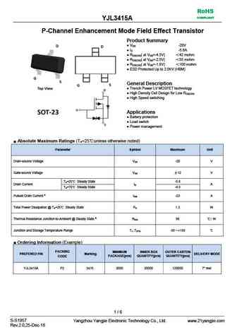
RoHS COMPLIANT YJL3415A P-Channel Enhancement Mode Field Effect Transistor Product Summary V -20V DS I -5.6A D R ( at V =-4.5V) 42 mohm DS(ON) GS R ( at V =-2.5V) 55 mohm DS(ON) GS R ( at V =-1.8V) 100 mohm DS(ON) GS ESD Protected Up to 2.0KV (HBM) General Description Trench Power LV MOSFET technology High Density Cell Des... See More ⇒
hm3415e.pdf
HM3415E P-Channel Enhancement Mode Power MOSFET Description The HM3415E uses advanced trench technology to provide excellent RDS(ON), low gate charge and operation with gate voltages as low as1.8V. This device is suitable for use as a load switch or in PWM applications .It is ESD protested. General Features VDS = -20V,ID =-4A Schematic diagram RDS(ON) ... See More ⇒
hpm3415.pdf
HPM3415 P-Channel MOSFETs -4.0A,-30V P P HPM3415 P-Channel Enhancement-Mode MOS FETs P-Channel Enhancement Features Mode MOS FETs -20V, -4.0A, RDS(ON)=35m @ VGS=-4.5V High dense cell design for extremely low RDS(ON) Rugged and reliable Lea... See More ⇒
irf3415.pdf
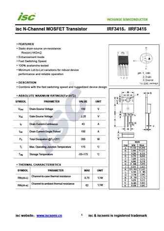
isc N-Channel MOSFET Transistor IRF3415 IIRF3415 FEATURES Static drain-source on-resistance RDS(on) 42m Enhancement mode Fast Switching Speed 100% avalanche tested Minimum Lot-to-Lot variations for robust device performance and reliable operation DESCRITION Combine with the fast switching speed and ruggedized device design ABSOLUTE MAXIMUM RATINGS(T =25 )... See More ⇒
irf3415l.pdf
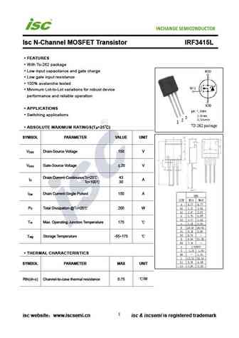
Isc N-Channel MOSFET Transistor IRF3415L FEATURES With To-262 package Low input capacitance and gate charge Low gate input resistance 100% avalanche tested Minimum Lot-to-Lot variations for robust device performance and reliable operation APPLICATIONS Switching applications ABSOLUTE MAXIMUM RATINGS(T =25 ) a SYMBOL PARAMETER VALUE UNIT V Drain-Source Voltage 150... See More ⇒
irf3415s.pdf
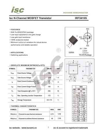
Isc N-Channel MOSFET Transistor IRF3415S FEATURES With To-263(D2PAK) package Low input capacitance and gate charge Low gate input resistance 100% avalanche tested Minimum Lot-to-Lot variations for robust device performance and reliable operation APPLICATIONS Switching applications ABSOLUTE MAXIMUM RATINGS(T =25 ) a SYMBOL PARAMETER VALUE UNIT V Drain-Source Volt... See More ⇒
2sk3415ls.pdf
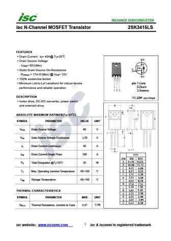
isc N-Channel MOSFET Transistor 2SK3415LS FEATURES Drain Current I = 40A@ T =25 D C Drain Source Voltage V = 60V(Min) DSS Static Drain-Source On-Resistance R = 17m (Max) @ V = 10V DS(on) GS 100% avalanche tested Minimum Lot-to-Lot variations for robust device performance and reliable operation DESCRIPTION motor drive, DC-DC converter, power switch and soleno... See More ⇒
irfp3415.pdf
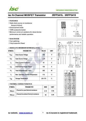
isc N-Channel MOSFET Transistor IRFP3415 IIRFP3415 FEATURES Static drain-source on-resistance RDS(on) 42m Enhancement mode 100% avalanche tested Minimum Lot-to-Lot variations for robust device performance and reliable operation DESCRITION Fast switching Fully Avalanche Rated ABSOLUTE MAXIMUM RATINGS(T =25 ) a SYMBOL PARAMETER VALUE UNIT V Drain-Source ... See More ⇒
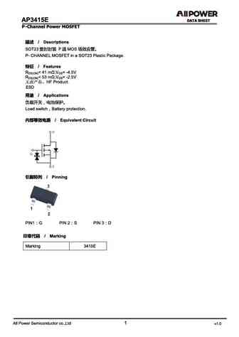
ap3415a.pdf
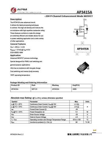
AP3415A -20V P-Channel Enhancement Mode MOSFET Description The AP3415A uses advanced trench It utilizes the latest processing techniques to achieve the high cell density and reduces the on-resistance with high repetitive avalanche rating. These features combine to make this design an extremely efficient and reliable device for use in power switching application and a wide var... See More ⇒
Detailed specifications: 1515 , G1601 , 2300 , 2301 , 2302 , 3035 , 3400 , 3401 , AO4468 , 6616 , 6703 , 6760 , 7080 , 8070 , 8680 , G29 , G33 .
Keywords - 3415 MOSFET specs
3415 cross reference
3415 equivalent finder
3415 pdf lookup
3415 substitution
3415 replacement
Can't find your MOSFET? Learn how to find a substitute transistor by analyzing voltage, current and package compatibility
🌐 : EN ES РУ

LIST
Last Update
MOSFET: ASB80R750E | ASB70R380E | ASB65R300E | ASB65R220E | ASB65R120EFD | ASB60R150E | ASA80R900E | ASA80R750E | ASA80R290E | ASA70R950E
Popular searches
2sb646 | 2sc1885 datasheet | 2sc2580 | 2sc710 | 2sc968 | 2sd217 | bdw93c equivalent | cs7n60f