18N10 Datasheet. Specs and Replacement
Type Designator: 18N10 📄📄
Type of Transistor: MOSFET
Type of Control Channel: N-Channel
Absolute Maximum Ratings
Pd ⓘ - Maximum Power Dissipation: 55 W
|Vds|ⓘ - Maximum Drain-Source Voltage: 100 V
|Vgs|ⓘ - Maximum Gate-Source Voltage: 20 V
|Id| ⓘ - Maximum Drain Current: 18 A
Tj ⓘ - Maximum Junction Temperature: 150 °C
Electrical Characteristics
tr ⓘ - Rise Time: 9.3 nS
Cossⓘ - Output Capacitance: 240 pF
RDSonⓘ - Maximum Drain-Source On-State Resistance: 0.07 Ohm
Package: TO252
📄📄 Copy
- MOSFET ⓘ Cross-Reference Search
18N10 datasheet
..1. Size:1693K goford
18n10.pdf 
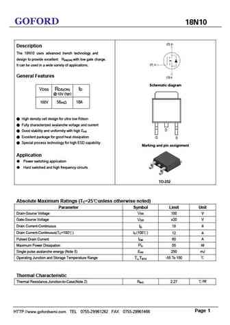
GOFORD 18N10 Description The 18N10 uses advanced trench technology and design to provide excellent RDS(ON) with low gate charge. It can be used in a wide variety of applications. General Features Schematic diagram VDSS RDS(ON) ID @ 10V (typ) 18A 100V 56m High density cell design for ultra low Rdson Fully characterized avalanche voltage and current Good st... See More ⇒
0.2. Size:439K infineon
bsc118n10ns8 bsc118n10nsg.pdf
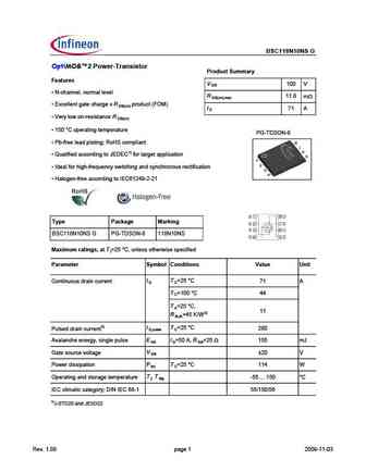
BSC118N10NS G OptiMOS 2 Power-Transistor Product Summary Features V 100 V DS N-channel, normal level R 11.8 m DS(on),max Excellent gate charge x R product (FOM) DS(on) I 71 A D Very low on-resistance R DS(on) 150 C operating temperature PG-TDSON-8 Pb-free lead plating; RoHS compliant Qualified according to JEDEC1) for target application Ide... See More ⇒
0.3. Size:570K infineon
ips118n10n.pdf
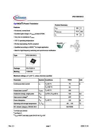
$& " " $;B1= '=- >5>?;= $=;0@/? &@99-=D Features 100 V DS R ( 492??6= ?@C>2= =6G6= 11.8 m DS(on) max R I46==6?E 82E6 492C86 I AC@5F4E !) ' DS(on) 75 A D R /6CJ =@H @? C6D DE2?46 DS(on) R U @A6C2E ?8 E6>A6C2EFC6 R *3 7C66 =625 A=2E ?8 , @#- 4@>A= 2?E 1) R + F2= 7 65 244@C5 ?8 E@ % 7@C E2C86E 2AA= 42E @? R $562= 7@C 9 89 7C6BF6?4J DH E49 ?8 2?5 DJ?49C@?@FD C64E 7 4... See More ⇒
0.4. Size:780K infineon
iauz18n10s5l420.pdf
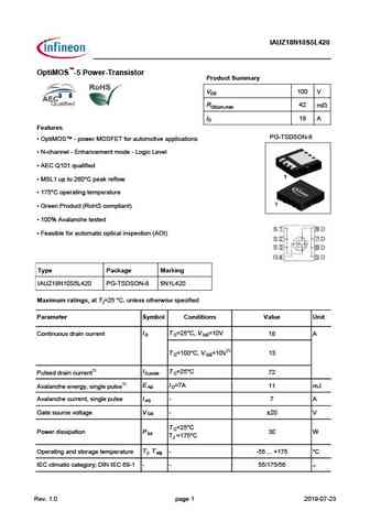
IAUZ18N10S5L420 OptiMOS -5 Power-Transistor Product Summary VDS 100 V RDS(on),max 42 mW ID 18 A Features PG-TSDSON-8 OptiMOS - power MOSFET for automotive applications N-channel - Enhancement mode - Logic Level AEC Q101 qualified 1 MSL1 up to 260 C peak reflow 175 C operating temperature 1 Green Product (RoHS compliant) 100% Avalanche tested ... See More ⇒
0.7. Size:1262K goford
18n10w.pdf
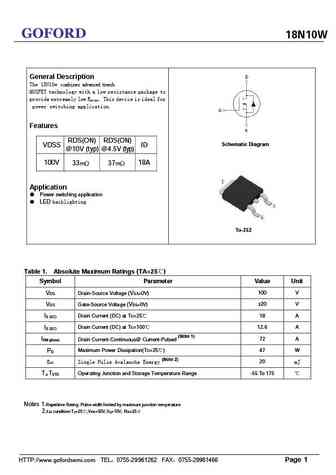
GOFORD 18N10W General Description The 18N10w combines advanced trench MOSFET technology with a low resistance package to provide extremely low R . This device is ideal for DS(ON) power switching application. Features RDS(ON) RDS(ON) Schematic Diagram VDSS ID @10V (typ) @4.5V (typ) 100V 33 m 37m 18A Application Power switching application LED backligh... See More ⇒
0.8. Size:714K hymexa
hyg018n10ns1b6.pdf
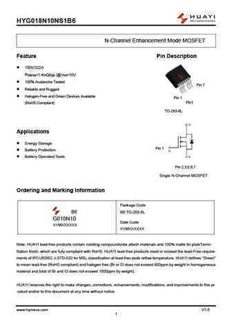
HYG018N10NS1B6 N-Channel Enhancement Mode MOSFET Feature Pin Description 100V/322A RDS(ON)=1.4m (typ.)@VGS=10V 100% Avalanche Tested Pin 7 Reliable and Rugged Halogen-Free and Green Devices Available Pin 1 Pin1 (RoHS Compliant) TO-263-6L TO-263-6L Applications Energy Storage Pin 1 Battery Protection Battery Operated Tools Pin 2... See More ⇒
0.9. Size:711K ncepower
ncep018n10ll.pdf
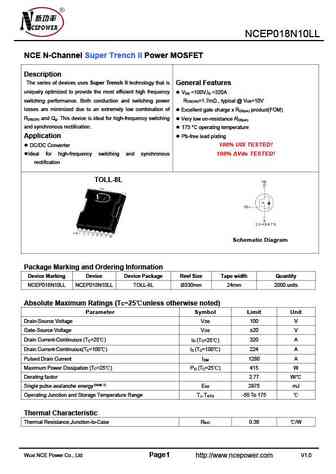
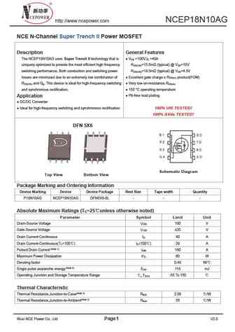
NCEP018N10LL NCE N-Channel Super Trench II Power MOSFET Description The series of devices uses Super Trench II technology that is General Features uniquely optimized to provide the most efficient high frequency V =100V,I =320A DS D switching performance. Both conduction and switching power R =1.7m , typical @ V =10V DS(ON) GS losses are minimized due to an extremely low combinat... See More ⇒
0.10. Size:294K ncepower
ncep18n10ar.pdf

http //www.ncepower.com NCEP18N10AR NCE N-Channel Super Trench II Power MOSFET Description General Features The NCEP18N10AR uses Super Trench II technology that is VDS =100V,ID =9.5A uniquely optimized to provide the most efficient high frequency RDS(ON)=19.2m (typical) @ VGS=10V switching performance. Both conduction and switching power RDS(ON)=23.0m (typical) @ VGS=4.5V l... See More ⇒
0.11. Size:735K ncepower
ncep18n10ak.pdf
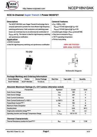
http //www.ncepower.com NCEP18N10AK NCE N-Channel Super Trench II Power MOSFET Description General Features The NCEP18N10AK uses Super Trench II technology that is V =100V,I =42A DS D uniquely optimized to provide the most efficient high frequency R =15.5m (typical) @ V =10V DS(ON) GS switching performance. Both conduction and switching power R =19.5m (typical) @ V =4.5V DS(ON) ... See More ⇒
0.12. Size:326K ncepower
ncep18n10aq.pdf
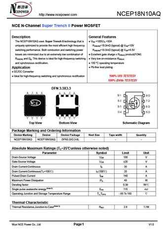
http //www.ncepower.com NCEP18N10AQ NCE N-Channel Super Trench II Power MOSFET Description General Features The NCEP18N10AQ uses Super Trench II technology that is VDS =100V,ID =35A uniquely optimized to provide the most efficient high frequency RDS(ON)=16.0m (typical) @ VGS=10V switching performance. Both conduction and switching power RDS(ON)=18.0m (typical) @ VGS=4.5V lo... See More ⇒
0.13. Size:874K ncepower
ncep18n10ag.pdf
http //www.ncepower.com NCEP18N10AG NCE N-Channel Super Trench II Power MOSFET Description General Features The NCEP18N10AG uses Super Trench II technology that is V =100V,I =40A DS D uniquely optimized to provide the most efficient high frequency R =15.5m (typical) @ V =10V DS(ON) GS switching performance. Both conduction and switching power R =19.5m (typical) @ V =4.5V DS(ON) ... See More ⇒
0.14. Size:614K stansontech
st18n10d.pdf
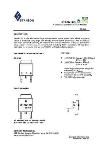
ST18N10D N Channel Enhancement Mode MOSFET 18.0A DESCRIPTION ST18N10D is the N-Channel logic enhancement mode power field effect transistor which is produced using high cell density, DMOS trench technology. The ST18N10D has been designed specially to improve the overall efficiency of DC/DC converters using either synchronous or conventional switching PWM controllers. It has been ... See More ⇒
0.15. Size:1387K cn agmsemi
agm18n10ap.pdf

AGM18N10AP Table 3. Electrical Characteristics (TJ=25 unless otherwise noted) Symbol Parameter Conditions Min Typ Max Unit On/Off States BV Drain-Source Breakdown Voltage V =0V I =250 A 100 -- -- V GS D DSS Zero Gate Voltage Drain Current V =100V,V =0V -- -- 1 A DS GS I DSS Gate-Body Leakage Current V = 20V,V =0V -- -- nA GS DS I GSS 100 V Gate Threshold Voltage V =V... See More ⇒
0.16. Size:1257K cn agmsemi
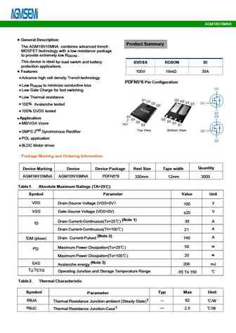
agm18n10mna.pdf
AGM18N10MNA Typical Performance Characteristics Vds Drain-Source Voltage (V) TJ-Junction Temperature( ) Figure 1 Output Characteristics Figure 4 Rdson-Junction Temperature Vgs Gate-Source Voltage (V) Qg Gate Charge (nC) Figure 2 Transfer Characteristics Figure 5 Gate Charge ID- Drain Current (A) Vsd Source-Drain Voltage (V) Figure 3 Rdson- Drain Current Figure 6 Source- Drain D... See More ⇒
0.17. Size:1219K cn agmsemi
agm18n10i.pdf
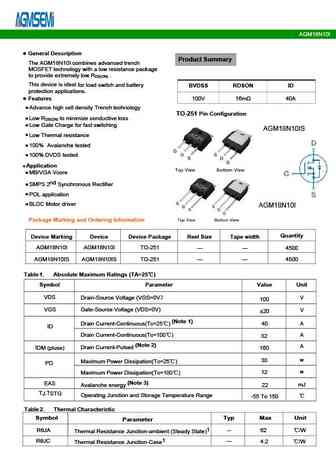
AGM18N10I Typical Performance Characteristics Figure 1. Output Characteristics Figure 2. Transfer Characteristics Figure 3. Drain-to-Source On Resistance Figure 4. Body Diode Forward Voltage vs Drain Current vs Source Current and Temperature Figure 5. Capacitance Characteristics Figure 6. Gate Charge Characteristics www.agm-mos.com 3 VER2.71 AGM18N10I Figure 13. Maximum Eff... See More ⇒
0.18. Size:1612K cn agmsemi
agm18n10a.pdf

AGM18N10A Table 3. Electrical Characteristics (TJ=25 unless otherwise noted) Symbol Parameter Conditions Min Typ Max Unit On/Off States BV Drain-Source Breakdown Voltage V =0V I =250 A 100 -- -- V GS D DSS Zero Gate Voltage Drain Current V =100V,V =0V -- -- 1 A DS GS I DSS Gate-Body Leakage Current V = 20V,V =0V -- -- nA GS DS I GSS 100 V Gate Threshold Voltage V =V ... See More ⇒
0.19. Size:1476K cn agmsemi
agm18n10s.pdf

AGM18N10S General Description Product Summary The AGM18N10S combines advanced trench MOSFET technology with a low resistance package to provide extremely low R . DS(ON) This device is ideal for load switch and battery BVDSS RDSON ID protection applications. Features 100V 17m 12A Advance high cell density Trench technology SOP8 Pin Configuration Low R to minimize... See More ⇒
0.20. Size:307K cn vanguard
vst018n10ms.pdf
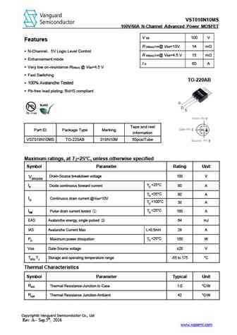
VST018N10MS 100V/60A N-Channel Advanced Power MOSFET V DS 100 V Features R DS(on),TYP@ VGS=10V 14 m N-Channel 5V Logic Level Control R DS(on),TYP@ VGS=4.5 V 15 m Enhancement mode I D 60 A Very low on-resistance RDS(on) @ VGS=4.5 V Fast Switching TO-220AB 100% Avalanche Tested Pb-free lead plating; RoHS compliant Tape and reel Part ID Pac... See More ⇒
0.21. Size:1002K cn hmsemi
hms18n10q.pdf
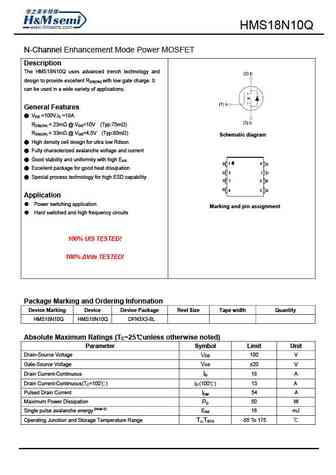
HMS18N10Q N-Channel Enhancement Mode Power MOSFET Description The HMS18N10Q uses advanced trench technology and design to provide excellent RDS(ON) with low gate charge. It can be used in a wide variety of applications. General Features VDS =100V,ID =18A RDS(ON) ... See More ⇒
0.22. Size:1354K cn hmsemi
hms18n10d.pdf
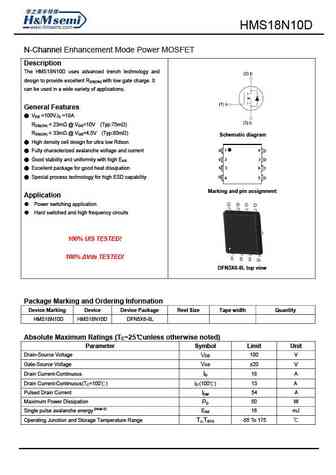
HMS18N10D N-Channel Enhancement Mode Power MOSFET Description The HMS18N10D uses advanced trench technology and design to provide excellent RDS(ON) with low gate charge. It can be used in a wide variety of applications. General Features VDS =100V,ID =18A RDS(ON) ... See More ⇒
0.23. Size:911K cn scilicon
sft018n100c3.pdf
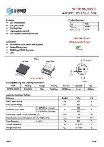
SFT018N100C3 N-MOSFET 100V, 1.55m , 320A Features Product Summary Low on resistance V 100V DS Low gate charge R 1.55m DS(on)typ. Fast switching I 320A D(Silicon Limited) High avalanche current Low reverse transfer capacitances 100% DVDS Tested Application 100% Avalanche Tested Brushed and BLDC Motor drive systems Battery Management D... See More ⇒
0.24. Size:1019K cn minos
mdt18n10d.pdf

100V N-Channel Power MOSFET DESCRIPTION The MDT18N10D uses advanced trench technology to provide excellent RDS(ON), low gate charge. It can be used in a wide variety of applications. Application Power switching application Hard switched and High frequency circuits Uninterruptible power supply Schematic diagram KEY CHARACTERISTICS V = 100V,I = 18A DS D R ... See More ⇒
Detailed specifications: G120N04, G120N04A, G15P04, G1815, G1816, G1825, 15P03, 16N10, TK10A60D, 2002A, 20P10, 21N06, 22N10, 2301H, 2301L, 25P06, 25P10
Keywords - 18N10 MOSFET specs
18N10 cross reference
18N10 equivalent finder
18N10 pdf lookup
18N10 substitution
18N10 replacement
Learn how to find the right MOSFET substitute. A guide to cross-reference, check specs and replace MOSFETs in your circuits.