FTK1016 Specs and Replacement
Type Designator: FTK1016
Type of Transistor: MOSFET
Type of Control Channel: N-Channel
Absolute Maximum Ratings
Pd ⓘ - Maximum Power Dissipation: 227 W
|Vds|ⓘ - Maximum Drain-Source Voltage: 100 V
|Vgs|ⓘ - Maximum Gate-Source Voltage: 20 V
|Id| ⓘ - Maximum Drain Current: 75 A
Tj ⓘ - Maximum Junction Temperature: 150 °C
Electrical Characteristics
tr ⓘ - Rise Time: 15.6 nS
Cossⓘ - Output Capacitance: 350 pF
RDSonⓘ - Maximum Drain-Source On-State Resistance: 0.016 Ohm
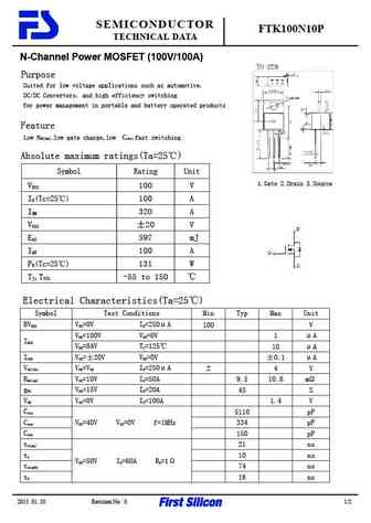
Package: TO220
FTK1016 substitution
- MOSFET ⓘ Cross-Reference Search
FTK1016 datasheet
ftk1016.pdf
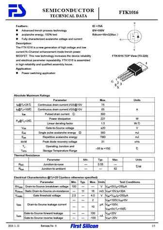
SEMICONDUCTOR FTK1016 TECHNICAL DATA Feathers ID =75A Advanced trench process technology BV=100V avalanche energy, 100% test Rdson=16m (Max. Fully characterized avalanche voltage and current Description The FTK1016 is a new generation of high voltage and low current N Channel enhancement mode trench power MOSFET. This new technology increases the device reliability ... See More ⇒
ftk1013.pdf
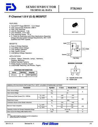
SEMICONDUCTOR FTK1013 TECHNICAL DATA P-Channel 1.8-V (G-S) MOSFET FEATURES TrenchFET Power MOSFET 1.8-V Rated Gate-Source ESD Protected 2000 V High-Side Switching Low On-Resistance 1.2 SOT-523 Low Threshold 0.8 V (typ) Fast Switching Speed 14 ns S- Prefix for Automotive and Other Applications Requiring Unique Site and Control Change Requirements; AEC-Q101 Qualified and... See More ⇒
ftk10n65p f dd.pdf

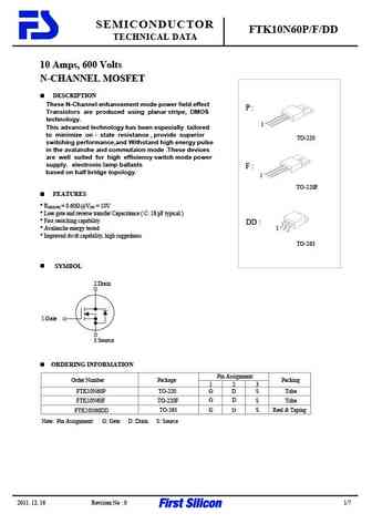
SEMICONDUCTOR FTK10N65P / F / DD TECHNICAL DATA 10 Amps, 650 Volts N-CHANNEL MOSFET DESCRIPTION These N-Channel enhancement mode power field effect P Transistors are produced using planar stripe, DMOS technology. 1 This advanced technology has been especially tailored to minimize on - state resistance , provide superior TO-220 switching performance,and Withstand high energy pul... See More ⇒
ftk1090.pdf
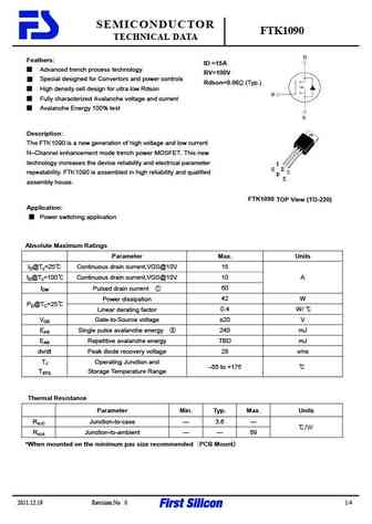
SEMICONDUCTOR FTK1090 TECHNICAL DATA Feathers ID =15A Advanced trench process technology BV=100V Special designed for Convertors and power controls Rdson=0.06 (Typ.) High density cell design for ultra low Rdson Fully characterized Avalanche voltage and current Avalanche Energy 100% test Description The FTK1090 is a new generation of high voltage an... See More ⇒
Detailed specifications: 2SK3674-01S , 2SK3674-01SJ , 2SK3899 , FTK9451 , FTK9452 , FTK03N10 , FTK100N10P , FTK1013 , TK10A60D , FTK1090 , FTK10N10 , FTK10N60DD , FTK10N60F , FTK10N60P , FTK8810 , FTK8810L , FTK8822 .
Keywords - FTK1016 MOSFET specs
FTK1016 cross reference
FTK1016 equivalent finder
FTK1016 pdf lookup
FTK1016 substitution
FTK1016 replacement
Learn how to find the right MOSFET substitute. A guide to cross-reference, check specs and replace MOSFETs in your circuits.
🌐 : EN ES РУ

LIST
Last Update
MOSFET: ASB80R750E | ASB70R380E | ASB65R300E | ASB65R220E | ASB65R120EFD | ASB60R150E | ASA80R900E | ASA80R750E | ASA80R290E | ASA70R950E
Popular searches
tip42c | 2sc2240 | bc547 transistor equivalent | 2sa1943 | tip41c datasheet | mje15032 | tip32c datasheet | mje15032g