FTK8810 Specs and Replacement
Type Designator: FTK8810
Type of Transistor: MOSFET
Type of Control Channel: N-Channel
Absolute Maximum Ratings
Pd ⓘ - Maximum Power Dissipation: 1.5 W
|Vds|ⓘ - Maximum Drain-Source Voltage: 20 V
|Vgs|ⓘ - Maximum Gate-Source Voltage: 12 V
|Id| ⓘ - Maximum Drain Current: 7 A
Tj ⓘ - Maximum Junction Temperature: 150 °C
Electrical Characteristics
tr ⓘ - Rise Time: 12.5 nS
RDSonⓘ - Maximum Drain-Source On-State Resistance: 0.02 Ohm
Package: TSSOP8
FTK8810 substitution
- MOSFET ⓘ Cross-Reference Search
FTK8810 datasheet
ftk8810.pdf
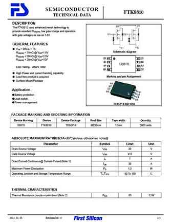
SEMICONDUCTOR FTK8810 TECHNICAL DATA DESCRIPTION The FTK8810 uses advanced trench technology to provide excellent RDS(ON), low gate charge and operation with gate voltages as low as 1.8V. GENERAL FEATURES VDS = 20V,ID = 7A Schematic diagram RDS(ON) ... See More ⇒
ftk8810l.pdf
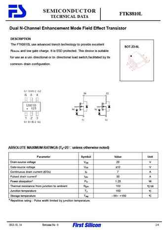
SEMICONDUCTOR FTK8810L TECHNICAL DATA Dual N-Channel Enhancement Mode Field Effect Transistor DESCRIPTION The FTK8810L use advanced trench technology to provide excellent SOT-23-6L RDS(ON) and low gate charge. It is ESD protected. This device is suitable for use as a uni-directional or bi-directional load switch,facilitated by its common-drain configuration. ABSOLUTE MAXIMUM RAT... See More ⇒
ftk8822.pdf
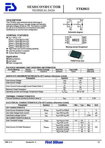
SEMICONDUCTOR FTK8822 TECHNICAL DATA D 1 D 2 DESCRIPTION The FTK8822 uses advanced trench technology to provide excellent RDS(ON), low gate charge and operation G 1 G 2 with gate voltages as low as 1.8V. This device is suitable for use as a uni-directional or bi-directional load switch, S 1 S 2 facilitated by its common-drain configuration. Schematic diagram GENERAL FEATURES... See More ⇒
Detailed specifications: FTK100N10P, FTK1013, FTK1016, FTK1090, FTK10N10, FTK10N60DD, FTK10N60F, FTK10N60P, 2SK3568, FTK8810L, FTK8822, FTK8N65DD, FTK8N65F, FTK8N65P, FTK8N80DD, FTK8N80F, FTK8N80P
Keywords - FTK8810 MOSFET specs
FTK8810 cross reference
FTK8810 equivalent finder
FTK8810 pdf lookup
FTK8810 substitution
FTK8810 replacement
Can't find your MOSFET? Learn how to find a substitute transistor by analyzing voltage, current and package compatibility
History: FTK9452 | FTK10N60F
🌐 : EN ES РУ

LIST
Last Update
MOSFET: ASD80R750E | ASD70R950E | ASD70R600E | ASD70R380E | ASD65R850E | ASD65R550E | ASD65R350E | ASD65R300E | ASD65R280E | ASD65R270E
Popular searches
tip32c datasheet | mje15032g | irf1404 | bc550 | irf9530 | 2n2222a transistor | irfp250 | irf640n datasheet