FTK3415L Specs and Replacement
Type Designator: FTK3415L
Type of Transistor: MOSFET
Type of Control Channel: P-Channel
Absolute Maximum Ratings
Pd ⓘ - Maximum Power Dissipation: 0.35 W
|Vds|ⓘ - Maximum Drain-Source Voltage: 20 V
|Vgs|ⓘ - Maximum Gate-Source Voltage: 8 V
|Id| ⓘ - Maximum Drain Current: 5.5 A
Tj ⓘ - Maximum Junction Temperature: 150 °C
Electrical Characteristics
tr ⓘ - Rise Time: 17 nS
Cossⓘ - Output Capacitance: 205 pF
RDSonⓘ - Maximum Drain-Source On-State Resistance: 0.05 Ohm
Package: SOT26
FTK3415L substitution
- MOSFET ⓘ Cross-Reference Search
FTK3415L datasheet
ftk3415l.pdf
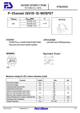
SEMICONDUCTOR FTK3415L TECHNICAL DATA P-Channel 20V(D-S) MOSFET ID V(BR)DSS RDS(on)MAX SOT-23-6L 50m @-4.5V -4.0A -20V 60m @-2.5V 73m @-1. 8V FEATURE APPLICATION Excellent RDS(ON), low gate charge,low gate voltage Load switch and in PWM applicatopns High power and current handing capability MARKING Equivalent Circuit PIN1 Maximum ratings (Ta=25 unless otherwise ... See More ⇒
ftk3415.pdf
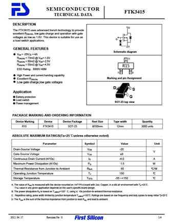
SEMICONDUCTOR FTK3415 TECHNICAL DATA DESCRIPTION D The FTK3415 uses advanced trench technology to provide excellent RDS(ON), low gate charge and operation with gate voltages as low as 1.8V. This device is suitable for use as G a load switch applications. S GENERAL FEATURES Schematic diagram VDS = -20V,ID =-4A RDS(ON) ... See More ⇒
ftk3400.pdf
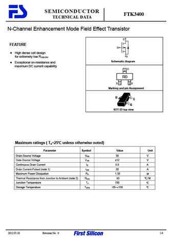
SEMICONDUCTOR FTK3400 TECHNICAL DATA N-Channel Enhancement Mode Field Effect Transistor D FEATURE G High dense cell design for extremely low R S DS(ON) Schematic diagram Exceptional on-resistance and maximum DC current capability D 3 R0 G 1 2 S Marking and pin Assignment SOT-23 top view Maximum ratings ( Ta=25 unless otherwise noted) Parameter Symbol Value Unit ... See More ⇒
ftk3404.pdf
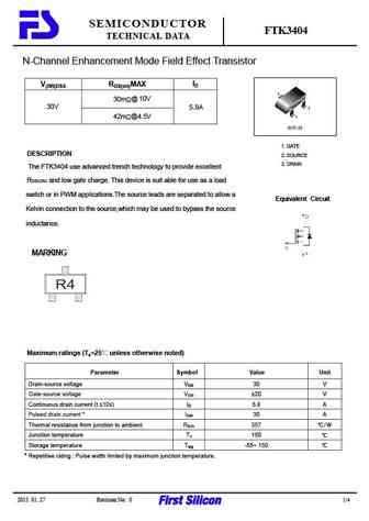
SEMICONDUCTOR FTK3404 TECHNICAL DATA N-Channel Enhancement Mode Field Effect Transistor ID V(BR)DSS RDS(on)MAX 3 30m @ 10V 30V 5.8A 2 1 42m @4.5V SOT 23 1. GATE DESCRIPTION 2. SOURCE 3. DRAIN The FTK3404 use advanced trench technology to provide excellent RDS(ON) and low gate charge. This device is suit able for use as a load switch or in PWM applications.The s... See More ⇒
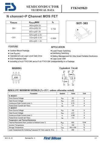
Detailed specifications: FTK3139K, FTK3341, FTK3400, FTK3401, FTK3404, FTK3407, FTK3407L, FTK3415, IRFZ44, FTK3439KD, FTK3443, FTK35N03PDFN33, FTK35N03PDFN56, FTK3610, FTK3615, FTK3620, FTK3N80I
Keywords - FTK3415L MOSFET specs
FTK3415L cross reference
FTK3415L equivalent finder
FTK3415L pdf lookup
FTK3415L substitution
FTK3415L replacement
Need a MOSFET replacement? Our guide shows you how to find a perfect substitute by comparing key parameters and specs
🌐 : EN ES РУ

LIST
Last Update
MOSFET: AUW033N08BG | AUW025N10 | AUR030N10 | AUR020N10 | AUR020N085 | AUR014N10 | AUP074N10 | AUP065N10 | AUP062N08BG | AUP060N08AG
Popular searches
c945 transistor equivalent | irfz44 datasheet | tip3055 transistor | irf530 datasheet | 2sc2625 | 2sc1815 transistor | 2sd718 | 2n3053 transistor