WNM2046B Specs and Replacement
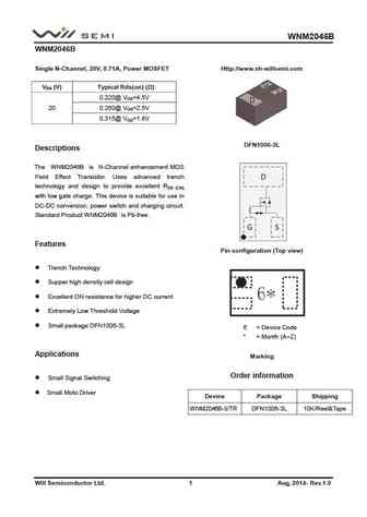
Type Designator: WNM2046B
Type of Transistor: MOSFET
Type of Control Channel: N-Channel
Absolute Maximum Ratings
Pd ⓘ
- Maximum Power Dissipation: 0.32 W
|Vds|ⓘ - Maximum Drain-Source Voltage: 20 V
|Vgs|ⓘ - Maximum Gate-Source Voltage: 5 V
|Id| ⓘ - Maximum Drain Current: 0.71 A
Electrical Characteristics
RDSonⓘ - Maximum Drain-Source On-State Resistance: 0.42 Ohm
Package: DFN1006-3
- MOSFET ⓘ Cross-Reference Search
WNM2046B datasheet
..1. Size:1480K willsemi
wnm2046b.pdf 

WNM2046B WNM2046B Single N-Channel, 20V, 0.71A, Power MOSFET Http //www.sh-willsemi.com G VDS (V) Typical Rds(on) ( ) S 0.220@ VGS=4.5V D 20 0.260@ VGS=2.5V 0.315@ VGS=1.8V DFN1006-3L Descriptions The WNM2046B is N-Channel enhancement MOS Field Effect Transistor. Uses advanced trench D technology and design to provide excellent RDS (ON) with low gate charge. This device is suit... See More ⇒
7.1. Size:1225K willsemi
wnm2046c.pdf 

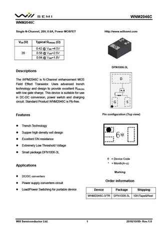
WNM2046C WNM2046C Single N-Channel, 20V, 0.6A, Power MOSFET Http //www.willsemi.com G V (V) Typical R ( ) DS DS(on) S D 0.42 @ V =4.5V GS 20 0.58 @ V =2.5V GS 0.84 @ V =1.8V GS DFN1006-3L Descriptions D The WPM2046C is N-Channel enhancement MOS Field Effect Transistor. Uses advanced trench technology and design to provide excellent R DS(ON) with low gate char... See More ⇒
7.2. Size:1062K willsemi
wnm2046.pdf 

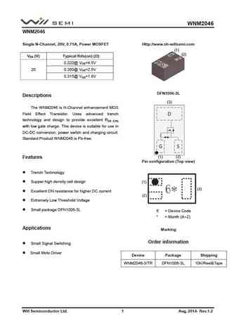
WNM2046 WNM2046 Single N-Channel, 20V, 0.71A, Power MOSFET Http //www.sh-willsemi.com (1) (2) G VDS (V) Typical Rds(on) ( ) S 0.220@ VGS=4.5V (3) D 20 0.260@ VGS=2.5V 0.315@ VGS=1.8V DFN1006-3L Descriptions (3) The WNM2046 is N-Channel enhancement MOS Field Effect Transistor. Uses advanced trench D technology and design to provide excellent RDS (ON) with low gate charge. Thi... See More ⇒
9.1. Size:909K willsemi
wnm2024.pdf 

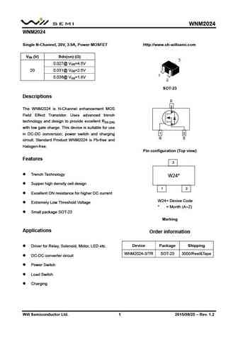
WNM2024 WNM2024 Single N-Channel, 20V, 3.9A, Power MOSFET Http //www.sh-willsemi.com VDS (V) Rds(on) ( ) 0.027@ VGS=4.5V 20 0.031@ VGS=2.5V 0.036@ VGS=1.8V SOT-23 Descriptions D 3 The WNM2024 is N-Channel enhancement MOS Field Effect Transistor. Uses advanced trench technology and design to provide excellent RDS (ON) with low gate charge. This device is suitable for us... See More ⇒
9.2. Size:1935K willsemi
wnm2072.pdf 

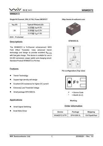
WNM2072 WNM2072 Single N-Channel, 20V, 0.71A, Power MOSFET Http //www.sh-willsemi.com G VDS (V) Typical Rds(on) ( ) S 0.220@ VGS=4.5V D 20 0.260@ VGS=2.5V 0.315@ VGS=1.8V ESD Protected DFN1006-3L Descriptions The WNM2072 is N-Channel enhancement MOS Field Effect Transistor. Uses advanced trench D technology and design to provide excellent RDS (ON) with low gate charge. This de... See More ⇒
9.3. Size:559K willsemi
wnm2030.pdf 

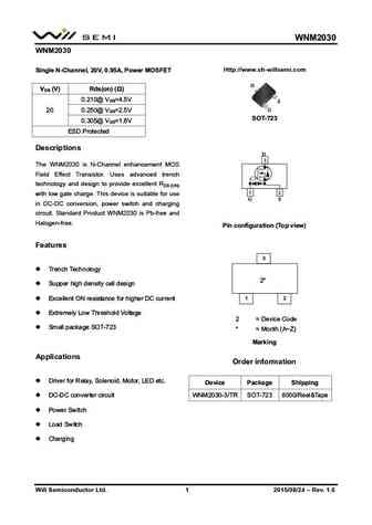
WNM2030 WNM2030 Http //www.sh-willsemi.com Single N-Channel, 20V, 0.95A, Power MOSFET D VDS (V) Rds(on) ( ) 0.210@ VGS=4.5V S G 20 0.250@ VGS=2.5V SOT-723 0.305@ VGS=1.8V ESD Protected Descriptions D 3 The WNM2030 is N-Channel enhancement MOS Field Effect Transistor. Uses advanced trench technology and design to provide excellent RDS (ON) 1 2 with low gate ch... See More ⇒
9.4. Size:440K willsemi
wnm2020.pdf 

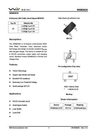
WNM2020 WNM2020 Http //www.sh-willsemi.com N-Channel, 20V, 0.90A, Small Signal MOSFET VDS (V) Rds(on) ( ) D 0.220@ VGS=4.5V 20 0.260@ VGS=2.5V S 0.320@ VGS=1.8V G SOT-23 Descriptions The WNM2020 is N-Channel enhancement MOS Field Effect Transistor. Uses advanced trench technology and design to provide excellent RDS (ON) D with low gate charge. This device is suitable for ... See More ⇒
9.5. Size:951K willsemi
wnm2077.pdf 

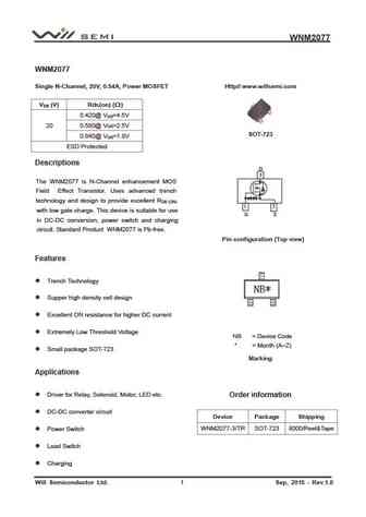
WNM2077 WNM2077 Single N-Channel, 20V, 0.54A, Power MOSFET Http// www.willsemi.com V (V) Rds(on) ( ) DS 0.420@ V =4.5V GS 20 0.580@ V =2.5V GS SOT-723 0.840@ V =1.8V GS ESD Protected Descriptions D 3 The WNM2077 is N-Channel enhancement MOS Field Effect Transistor. Uses advanced trench technology and design to provide excellent R DS (ON) 1 2 with low gate charge. This devi... See More ⇒
9.6. Size:389K willsemi
wnm2016.pdf 

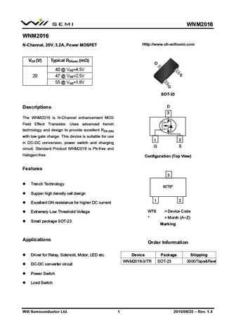
WNM2016 WNM2016 Http //www.sh-willsemi.com N-Channel, 20V, 3.2A, Power MOSFET VDS (V) Typical RDS(on) (m ) D 40 @ VGS=4.5V S 20 47 @ VGS=2.5V 55 @ VGS=1.8V G SOT-23 D Descriptions 3 The WNM2016 is N-Channel enhancement MOS Field Effect Transistor. Uses advanced trench technology and design to provide excellent RDS (ON) with low gate charge. This device is suitable ... See More ⇒
9.7. Size:872K willsemi
wnm2016a.pdf 

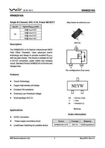
WNM2016A WNM2016A Single N-Channel, 20V, 4.7A, Power MOSFET Http //www.sh-willsemi.com V (V) Typical R (m ) DS DS(on) 33@ V =4.5V GS 39@ V =3.1V GS 20 44@ V =2.5V GS 66@ V =1.8V GS SOT-23 Description D 3 The WNM2016A is N-Channel enhancement MOS Field Effect Transistor. Uses advanced trench technology and design to provide excellent R DS(ON) with low gate cha... See More ⇒
9.8. Size:502K willsemi
wnm2021.pdf 

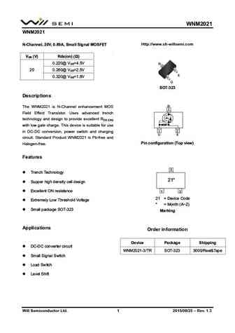
WNM2021 WNM2021 Http //www.sh-willsemi.com N-Channel, 20V, 0.89A, Small Signal MOSFET VDS (V) Rds(on) ( ) 0.220@ VGS=4.5V D 20 0.260@ VGS=2.5V S 0.320@ VGS=1.8V G SOT-323 Descriptions D The WNM2021 is N-Channel enhancement MOS 3 Field Effect Transistor. Uses advanced trench technology and design to provide excellent RDS (ON) with low gate charge. This device is suitable... See More ⇒
9.9. Size:393K tysemi
wnm2024.pdf 

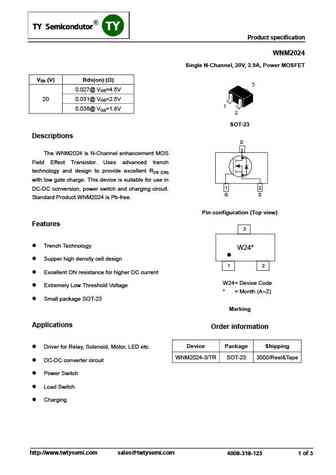
Product specification WNM2024 Single N-Channel, 20V, 3.9A, Power MOSFET VDS (V) Rds(on) ( ) 0.027@ VGS=4.5V 20 0.031@ VGS=2.5V 0.036@ VGS=1.8V SOT-23 Descriptions D 3 The WNM2024 is N-Channel enhancement MOS Field Effect Transistor. Uses advanced trench technology and design to provide excellent RDS (ON) with low gate charge. This device is suitable for use in 1 2 DC... See More ⇒
9.10. Size:136K tysemi
wnm2034.pdf 

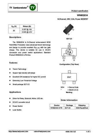
Product specification WNM2034 N-Channel, 20V, 3.6A, Power MOSFET VDS (V) Rdson ( ) 0.037 @ 10V 20 0.045 @ 4.5V Descriptions SOT-23 The WNM2034 is N-Channel enhancement MOS D Field Effect Transistor. Uses advanced trench technology 3 and design to provide excellent RDS (ON) with low gate charge. This device is suitable for use in DC-DC conversion and power switch application... See More ⇒
9.11. Size:124K tysemi
wnm2027.pdf 

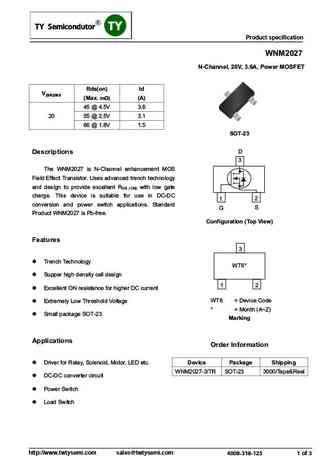
Product specification WNM2027 N-Channel, 20V, 3.6A, Power MOSFET Rds(on) Id V(BR)DSS (Max. m ) (A) 45 @ 4.5V 3.6 20 55 @ 2.5V 3.1 66 @ 1.8V 1.5 SOT-23 D Descriptions 3 The WNM2027 is N-Channel enhancement MOS Field Effect Transistor. Uses advanced trench technology and design to provide excellent RDS (ON) with low gate charge. This device is suitable for use in DC-DC ... See More ⇒
9.12. Size:442K tysemi
wnm2025.pdf 

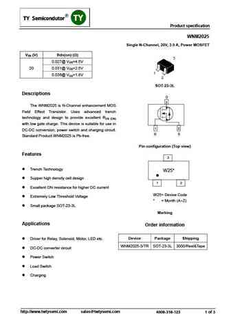
Product specification WNM2025 Single N-Channel, 20V, 3.9 A, Power MOSFET VDS (V) Rds(on) ( ) 0.027@ VGS=4.5V 20 0.031@ VGS=2.5V 0.036@ VGS=1.8V SOT-23-3L Descriptions D 3 The WNM2025 is N-Channel enhancement MOS Field Effect Transistor. Uses advanced trench technology and design to provide excellent RDS (ON) with low gate charge. This device is suitable for use in 1 2 ... See More ⇒
9.13. Size:167K tysemi
wnm2020.pdf 

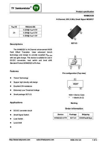
Product specification WNM2020 N-Channel, 20V, 0.90A, Small Signal MOSFET VDS (V) Rds(on) ( ) 0.220@ VGS=4.5V 20 0.260@ VGS=2.5V 0.320@ VGS=1.8V SOT-23 Descriptions The WNM2020 is N-Channel enhancement MOS Field Effect Transistor. Uses advanced trench technology and design to provide excellent RDS (ON) D 3 with low gate charge. This device is suitable for use in DC-DC convers... See More ⇒
9.14. Size:388K tysemi
wnm2023.pdf 

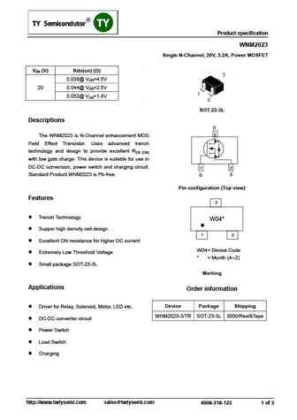
Product specification WNM2023 Single N-Channel, 20V, 3.2A, Power MOSFET VDS (V) Rds(on) ( ) 0.038@ VGS=4.5V 20 0.044@ VGS=2.5V 0.052@ VGS=1.8V SOT-23-3L Descriptions D 3 The WNM2023 is N-Channel enhancement MOS Field Effect Transistor. Uses advanced trench technology and design to provide excellent RDS (ON) with low gate charge. This device is suitable for use in DC-DC... See More ⇒
9.15. Size:99K tysemi
wnm2016.pdf 

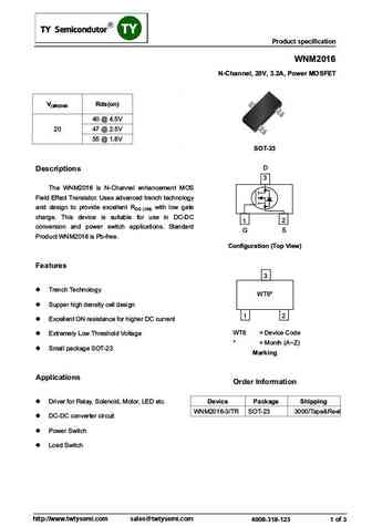
Product specification WNM2016 N-Channel, 20V, 3.2A, Power MOSFET V(BR)DSS Rds(on) 40 @ 4.5V 20 47 @ 2.5V 55 @ 1.8V SOT-23 D Descriptions 3 The WNM2016 is N-Channel enhancement MOS Field Effect Transistor. Uses advanced trench technology and design to provide excellent RDS (ON) with low gate charge. This device is suitable for use in DC-DC 2 1 conversion and power swit... See More ⇒
9.16. Size:1282K kexin
wnm2020.pdf 

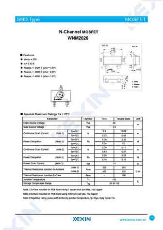
SMD Type MOSFET N-Channel MOSFET WNM2020 SOT-23 Unit mm +0.1 2.9 -0.1 +0.1 0.4 -0.1 3 Features VDS (V) = 20V ID = 0.83 A 1 2 RDS(ON) 310m (VGS = 4.5V) +0.1 +0.05 0.95-0.1 0.1-0.01 +0.1 1.9-0.1 RDS(ON) 360m (VGS = 2.5V) RDS(ON) 460m (VGS = 1.8V) 1. Gate 2. Source D 3. Drain 3 1 2 G S Absolute Maximum Ratings Ta = 2... See More ⇒
9.17. Size:431K slkor
wnm2021.pdf 

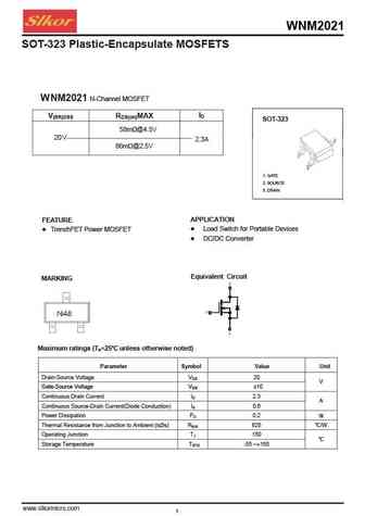
WNM2021 SOT-323 Plastic-Encapsulate MOSFETS W NM2021 N-Channel MOSFET ID V(BR)DSS RDS(on)MAX SOT-323 58m @4.5V 20 V 2.3A @2.5V 86m 1. GATE 2. SOURCE 3. DRAIN APPLICATION FEATURE Load Switch for Portable Devices TrenchFET Power MOSFET DC/DC Converter Equivalent Circuit MARKING Maximum ratings (Ta=25 unless otherwise noted) Parameter Symbol Value... See More ⇒
9.18. Size:1478K cn vbsemi
wnm2016-3.pdf 

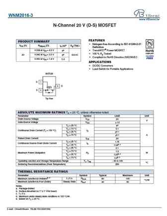
WNM2016-3 www.VBsemi.tw N-Channel 20 V (D-S) MOSFET FEATURES PRODUCT SUMMARY Halogen-free According to IEC 61249-2-21 VDS (V) RDS(on) ( ) ID (A)e Qg (Typ.) Definition 0.028 at VGS = 4.5 V TrenchFET Power MOSFET 6a 100 % Rg Tested 20 0.042 at VGS = 2.5 V 6a 8.8 nC Compliant to RoHS Directive 2002/95/EC 0.050 at VGS = 1.8 V 5.6 APPLICATIONS DC/DC... See More ⇒
9.19. Size:911K cn vbsemi
wnm2020-3.pdf 

WNM2020-3 www.VBsemi.tw N-Channel 20 V (D-S) MOSFET FEATURES PRODUCT SUMMARY Halogen-free According to IEC 61249-2-21 VDS (V) RDS(on) ( ) ID (A)e Qg (Typ.) Definition 0.028 at VGS = 4.5 V TrenchFET Power MOSFET 6a 100 % Rg Tested 20 0.042 at VGS = 2.5 V 6a 8.8 nC Compliant to RoHS Directive 2002/95/EC 0.050 at VGS = 1.8 V 5.6 APPLICATIONS DC/DC... See More ⇒
9.20. Size:844K cn vbsemi
wnm2021.pdf 

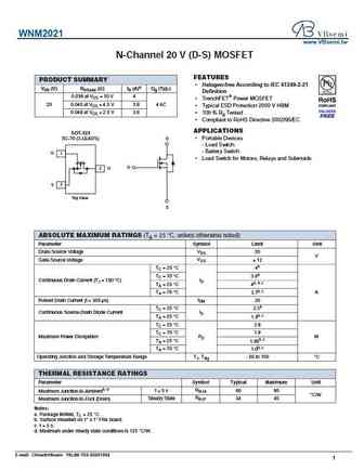
WNM2021 www.VBsemi.tw N-Channel 20 V (D-S) MOSFET FEATURES PRODUCT SUMMARY Halogen-free According to IEC 61249-2-21 VDS (V) RDS(on) ( )ID (A)a Qg (Typ.) Definition 0.036 at VGS = 10 V 4 TrenchFET Power MOSFET 20 0.040 at VGS = 4.5 V 3.8 4 nC Typical ESD Protection 2000 V HBM 0.048 at VGS = 2.5 V 3.6 100 % Rg Tested Compliant to RoHS Directive 2002/95/EC A... See More ⇒
Detailed specifications: WNM12N65, WNM12N65F, WNM2016, WNM2020, WNM2021, WNM2024, WNM2030, WNM2046, IRF830, WNM2072, WNM3003, WNM3008, WNM3011, WNM3013, WNM3017, WNM4001, WNM4002
Keywords - WNM2046B MOSFET specs
WNM2046B cross reference
WNM2046B equivalent finder
WNM2046B pdf lookup
WNM2046B substitution
WNM2046B replacement
Need a MOSFET replacement?
Our guide shows you how to find a perfect substitute by comparing key parameters and specs
