NCE2305A Specs and Replacement
Type Designator: NCE2305A
Type of Transistor: MOSFET
Type of Control Channel: P-Channel
Absolute Maximum Ratings
Pd ⓘ
- Maximum Power Dissipation: 1.25 W
|Vds|ⓘ - Maximum Drain-Source Voltage: 30 V
|Vgs|ⓘ - Maximum Gate-Source Voltage: 20 V
|Id| ⓘ - Maximum Drain Current: 5.4 A
Tj ⓘ - Maximum Junction Temperature: 150 °C
Electrical Characteristics
tr ⓘ - Rise Time: 4 nS
Cossⓘ -
Output Capacitance: 150 pF
RDSonⓘ - Maximum Drain-Source On-State Resistance: 0.055 Ohm
Package: SOT23
- MOSFET ⓘ Cross-Reference Search
NCE2305A datasheet
..1. Size:308K ncepower
nce2305a.pdf 
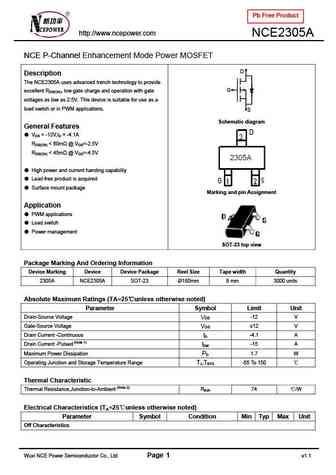
Pb Free Product http //www.ncepower.com NCE2305A NCE P-Channel Enhancement Mode Power MOSFET D Description The NCE2305A uses advanced trench technology to provide G excellent RDS(ON), low gate charge and operation with gate voltages as low as 2.5V. This device is suitable for use as a load switch or in PWM applications. S Schematic diagram General Features VDS = -12V,... See More ⇒
..2. Size:1748K cn vbsemi
nce2305a.pdf
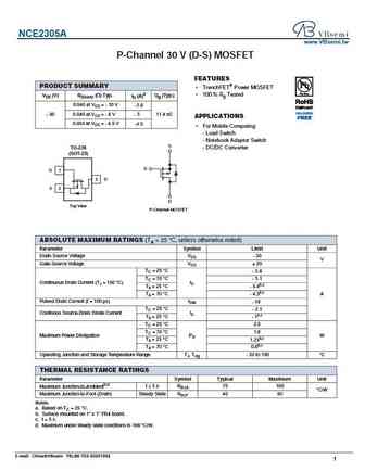
NCE2305A www.VBsemi.tw P-Channel 30 V (D-S) MOSFET FEATURES PRODUCT SUMMARY TrenchFET Power MOSFET 100 % Rg Tested VDS (V) RDS(on) ( ) Typ. ID (A)a Qg (Typ.) 0.046 at VGS = - 10 V - 5.6 0.049 at VGS = - 6 V - 5 11.4 nC - 30 APPLICATIONS 0.054 at VGS = - 4.5 V -4.5 For Mobile Computing - Load Switch - Notebook Adaptor Switch S TO-236 - DC/DC Converter (SOT-23... See More ⇒
7.1. Size:335K ncepower
nce2305.pdf
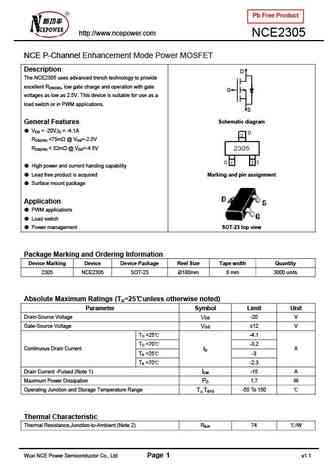
Pb Free Product http //www.ncepower.com NCE2305 NCE P-Channel Enhancement Mode Power MOSFET Description D The NCE2305 uses advanced trench technology to provide excellent RDS(ON), low gate charge and operation with gate G voltages as low as 2.5V. This device is suitable for use as a load switch or in PWM applications. S Schematic diagram General Features VDS = -20V,ID... See More ⇒
8.1. Size:262K ncepower
nce2301a.pdf
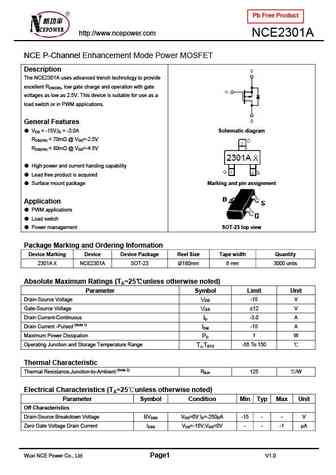
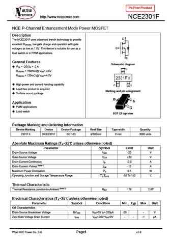
Pb Free Product http //www.ncepower.com NCE2301A NCE P-Channel Enhancement Mode Power MOSFET Description The NCE2301A uses advanced trench technology to provide excellent RDS(ON), low gate charge and operation with gate voltages as low as 2.5V. This device is suitable for use as a load switch or in PWM applications. General Features VDS = -15V,ID = -3.0A Schematic diagram ... See More ⇒
8.2. Size:257K ncepower
nce2301c.pdf

Pb Free Product http //www.ncepower.com NCE2301C NCE P-Channel Enhancement Mode Power MOSFET Description D The NCE2301C uses advanced trench technology to provide excellent RDS(ON), low gate charge and operation with gate G voltages as low as 1.8V. This device is suitable for use as a load switch or in PWM applications. S General Features Schematic diagram VDS = -15V,... See More ⇒
8.3. Size:330K ncepower
nce2301e.pdf
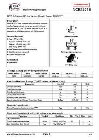
Pb Free Product http //www.ncepower.com NCE2301E NCE P-Channel Enhancement Mode Power MOSFET Description The NCE2301E uses advanced trench technology to provide excellent RDS(ON), low gate charge and operation with gate voltages as low as 2.5V. This device is suitable for use as a load switch or in PWM applications .It is ESD protested. Schematic diagram General Features ... See More ⇒
8.4. Size:350K ncepower
nce2309.pdf
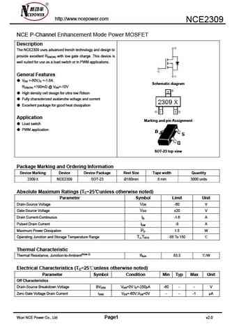
http //www.ncepower.com NCE2309 NCE P-Channel Enhancement Mode Power MOSFET Description The NCE2309 uses advanced trench technology and design to provide excellent RDS(ON) with low gate charge .This device is well suited for use as a load switch or in PWM applications. General Features VDS =-60V,ID =-1.6A Schematic diagram RDS(ON) ... See More ⇒
8.5. Size:344K ncepower
nce2304.pdf
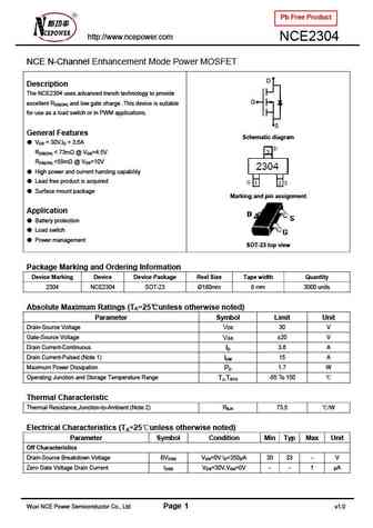
Pb Free Product http //www.ncepower.com NCE2304 NCE N-Channel Enhancement Mode Power MOSFET D Description The NCE2304 uses advanced trench technology to provide G excellent RDS(ON) and low gate charge .This device is suitable for use as a load switch or in PWM applications. S General Features Schematic diagram VDS = 30V,ID = 3.6A RDS(ON) ... See More ⇒
8.6. Size:234K ncepower
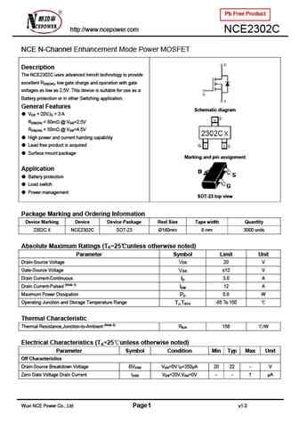
nce2302.pdf
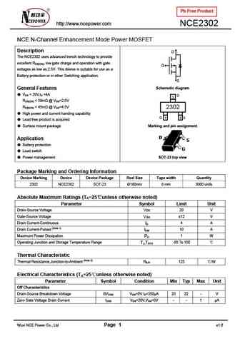
Pb Free Product http //www.ncepower.com NCE2302 NCE N-Channel Enhancement Mode Power MOSFET Description D The NCE2302 uses advanced trench technology to provide excellent RDS(ON), low gate charge and operation with gate G voltages as low as 2.5V. This device is suitable for use as a Battery protection or in other Switching application. S Schematic diagram General Features ... See More ⇒
8.7. Size:329K ncepower
nce2303.pdf
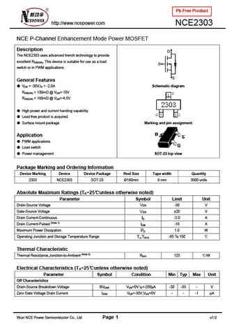
Pb Free Product http //www.ncepower.com NCE2303 NCE P-Channel Enhancement Mode Power MOSFET Description D The NCE2303 uses advanced trench technology to provide excellent RDS(ON), This device is suitable for use as a load G switch or in PWM applications. S General Features VDS = -30V,ID = -2.0A Schematic diagram RDS(ON) ... See More ⇒
8.8. Size:637K ncepower
nce2308x.pdf
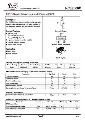
http //www.ncepower.com NCE2308X NCE N-Channel Enhancement Mode Power MOSFET D Description The NCE2308X uses advanced trench technology to provide G excellent R , low gate charge. This device is suitable for DS(ON) use as a Battery protection or in other switching application. S Schematic Diagram General Features V =60V,I =3A DS D R ... See More ⇒
8.9. Size:242K ncepower
nce2302c.pdf
Pb Free Product http //www.ncepower.com NCE2302C NCE N-Channel Enhancement Mode Power MOSFET Description The NCE2302C uses advanced trench technology to provide excellent RDS(ON), low gate charge and operation with gate voltages as low as 2.5V. This device is suitable for use as a Battery protection or in other Switching application. General Features Schematic diagram VD... See More ⇒
8.10. Size:241K ncepower
nce2301.pdf
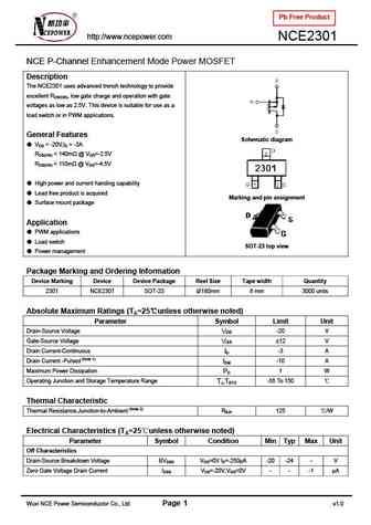
Pb Free Product http //www.ncepower.com NCE2301 NCE P-Channel Enhancement Mode Power MOSFET Description The NCE2301 uses advanced trench technology to provide excellent RDS(ON), low gate charge and operation with gate voltages as low as 2.5V. This device is suitable for use as a load switch or in PWM applications. General Features Schematic diagram VDS = -20V,ID = -3A ... See More ⇒
8.11. Size:261K ncepower
nce2301f.pdf
Pb Free Product http //www.ncepower.com NCE2301F NCE P-Channel Enhancement Mode Power MOSFET Description D The NCE2301F uses advanced trench technology to provide excellent RDS(ON), low gate charge and operation with gate G voltages as low as 1.8V. This device is suitable for use as a load switch or in PWM applications. S General Features Schematic diagram VDS = -20V,... See More ⇒
8.12. Size:249K ncepower
nce2301d.pdf

Pb Free Product http //www.ncepower.com NCE2301D NCE P-Channel Enhancement Mode Power MOSFET Description D The NCE2301D uses advanced trench technology to provide excellent RDS(ON), low gate charge and operation with gate G voltages as low as 1.8V. This device is suitable for use as a load switch or in PWM applications. S General Features Schematic diagram VDS = -20V,... See More ⇒
8.13. Size:245K ncepower
nce2302b.pdf
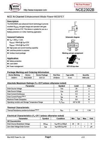
Pb Free Product http //www.ncepower.com NCE2302B NCE N-Channel Enhancement Mode Power MOSFET Description The NCE2302B uses advanced trench technology to provide excellent RDS(ON), low gate charge and operation with gate voltages as low as 2.5V. This device is suitable for use as a Battery protection or in other Switching application. Schematic diagram General Features VD... See More ⇒
8.14. Size:250K ncepower
nce2301b.pdf

Pb Free Product http //www.ncepower.com NCE2301B NCE P-Channel Enhancement Mode Power MOSFET Description D The NCE2301B uses advanced trench technology to provide excellent RDS(ON), low gate charge and operation with gate G voltages as low as 1.8V. This device is suitable for use as a load switch or in PWM applications. S General Features Schematic diagram VDS = -20V,... See More ⇒
Detailed specifications: SI4946BEY-T1, CS6N70FA9H, SMC3407S, CS6N80A0H, SI9945AEY-T1-E3, SI9945BDY-T1, SI9945DY, CS6N90A8H, 2SK3568, NCE3007S, MTD6P10ET4, MMSF7P03HDR2G, CS730A8H, SPN3400S23RG, CS730FA9H, CS730FA9RD, CS740A0H
Keywords - NCE2305A MOSFET specs
NCE2305A cross reference
NCE2305A equivalent finder
NCE2305A pdf lookup
NCE2305A substitution
NCE2305A replacement
Can't find your MOSFET?
Learn how to find a substitute transistor by analyzing voltage, current and package compatibility
