TK40P04M Specs and Replacement
Type Designator: TK40P04M
Type of Transistor: MOSFET
Type of Control Channel: N-Channel
Absolute Maximum Ratings
Pd ⓘ - Maximum Power Dissipation: 312 W
|Vds|ⓘ - Maximum Drain-Source Voltage: 40 V
|Vgs|ⓘ - Maximum Gate-Source Voltage: 25 V
|Id| ⓘ - Maximum Drain Current: 85 A
Tj ⓘ - Maximum Junction Temperature: 150 °C
Electrical Characteristics
tr ⓘ - Rise Time: 11 nS
Cossⓘ - Output Capacitance: 550 pF
RDSonⓘ - Maximum Drain-Source On-State Resistance: 0.0064 Ohm
Package: TO252
TK40P04M substitution
- MOSFET ⓘ Cross-Reference Search
TK40P04M datasheet
tk40p04m.pdf
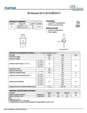
TK40P04M www.VBsemi.tw N-Channel 40-V (D-S) MOSFET FEATURES PRODUCT SUMMARY TrenchFET Power MOSFET VDS (V) RDS(on) ( ) ID (A)a, c Qg (Typ.) 100 % Rg and UIS Tested RoHS 0.0050 at VGS = 10 V 85 COMPLIANT 40 80 nC 0.0065 at VGS = 4.5 V 70 APPLICATIONS Synchronous Rectification Power Supplies D TO-252 G G D S S N-Channel MOSFET ABSOLUTE MAXIMUM RA... See More ⇒
tk40p04m1.pdf
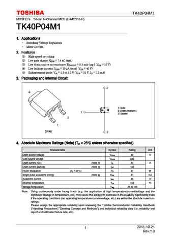
TK40P04M1 MOSFETs Silicon N-Channel MOS (U-MOS -H) TK40P04M1 TK40P04M1 TK40P04M1 TK40P04M1 1. Applications 1. Applications 1. Applications 1. Applications Switching Voltage Regulators Motor Drivers 2. Features 2. Features 2. Features 2. Features (1) High-speed switching (2) Low gate charge QSW = 7.4 nC (typ.) (3) Low drain-source on-resistance RDS(ON) = 8.5 m (t... See More ⇒
ftk40p04d.pdf
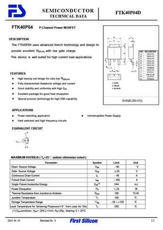
SEMICONDUCTOR FTK40P04D TECHNICAL DATA FTK40P04 P-Channel Power MOSFET A I DESCRIPTION C J The FTK40P04 uses advanced trench technology and design to provide excellent RDS(ON) with low gate charge. DIM MILLIMETERS A 6 50 0 2 B 5 60 0 2 This device is well suited for high current load applications. C 5 20 0 2 D 1 50 0 2 E 2 70 0 2 F 2 30 0 1 H H 1 00 MA... See More ⇒
tk40p03m1.pdf
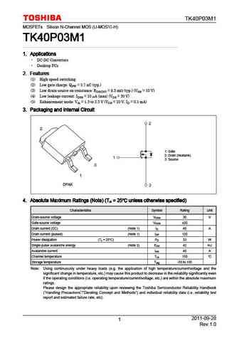
TK40P03M1 MOSFETs Silicon N-Channel MOS (U-MOS -H) TK40P03M1 TK40P03M1 TK40P03M1 TK40P03M1 1. Applications 1. Applications 1. Applications 1. Applications DC-DC Converters Desktop PCs 2. Features 2. Features 2. Features 2. Features (1) High-speed switching (2) Low gate charge QSW = 5.7 nC (typ.) (3) Low drain-source on-resistance RDS(ON) = 8.3 m (typ.) (VGS = 10... See More ⇒
Detailed specifications: CS8N50A8R, CS8N50FA9R, CS8N60A8D, VB1101M, CS8N60ARD, TP0610K-T1, TPC8103, TPC8104, IRF640, CS8N70FA9H2-G, CS8N80A8D, CS8N80A8H, VB1330, CS8N80FA9H, CS8N90A8, CS8N90FA9, VB162K
Keywords - TK40P04M MOSFET specs
TK40P04M cross reference
TK40P04M equivalent finder
TK40P04M pdf lookup
TK40P04M substitution
TK40P04M replacement
Can't find your MOSFET? Learn how to find a substitute transistor by analyzing voltage, current and package compatibility
🌐 : EN ES РУ

LIST
Last Update
MOSFET: ASU70R600E | ASU65R850E | ASU65R550E | ASU65R350E | ASR65R120EFD | ASR65R046EFD | ASQ65R046EFD | ASM65R280E | ASM60R330E | ASE70R950E
Popular searches
b1560 | 2sa1695 | a1175 transistor | 2sc1678 | irf4115 | 2sc828 replacement | 2sd669 datasheet | c102 transistor