IRF711 Specs and Replacement
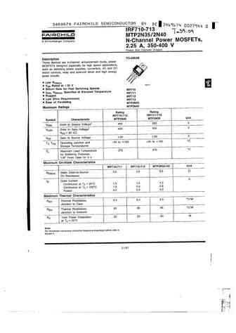
Type Designator: IRF711
Type of Transistor: MOSFET
Type of Control Channel: N-Channel
Absolute Maximum Ratings
Pd ⓘ
- Maximum Power Dissipation: 20 W
|Vds|ⓘ - Maximum Drain-Source Voltage: 350 V
|Vgs|ⓘ - Maximum Gate-Source Voltage: 20 V
|Id| ⓘ - Maximum Drain Current: 1.5 A
Tj ⓘ - Maximum Junction Temperature: 150 °C
Electrical Characteristics
tr ⓘ - Rise Time: 20 max nS
Cossⓘ -
Output Capacitance: 50 max pF
RDSonⓘ - Maximum Drain-Source On-State Resistance: 3.6 Ohm
Package: TO220AB
- MOSFET ⓘ Cross-Reference Search
IRF711 datasheet
9.1. Size:169K 1
irf7103q.pdf 

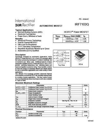
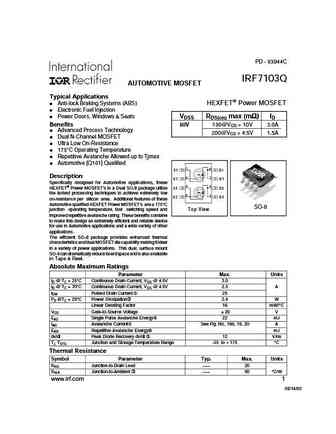
PD - 93944C IRF7103Q AUTOMOTIVE MOSFET Typical Applications Anti-lock Braking Systems (ABS) HEXFET Power MOSFET Electronic Fuel Injection ) ) ) ) Power Doors, Windows & Seats VDSS RDS(on) max (m ) ID Benefits 50V 130@VGS = 10V 3.0A Advanced Process Technology 200@VGS = 4.5V 1.5A Dual N-Channel MOSFET Ultra Low On-Resistance 175 C Operating Temperature R... See More ⇒
9.2. Size:402K 1
auirf7103q.pdf 

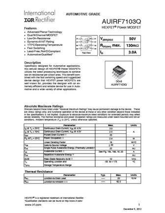
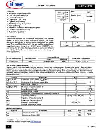
AUTOMOTIVE GRADE AUIRF7103Q HEXFET Power MOSFET Features l Advanced Planar Technology l Dual N Channel MOSFET 1 8 l Low On-Resistance S1 D1 V(BR)DSS 50V 2 7 l Dynamic dV/dT Rating G1 D1 3 6 l 175 C Operating Temperature S2 D2 RDS(on) max. 130m 4 5 l Fast Switching G2 D2 l Lead-Free, RoHS Compliant ID Top View 3.0A l Automotive Qualified* Description Specifically d... See More ⇒
9.3. Size:607K 1
irf7105q.pdf 

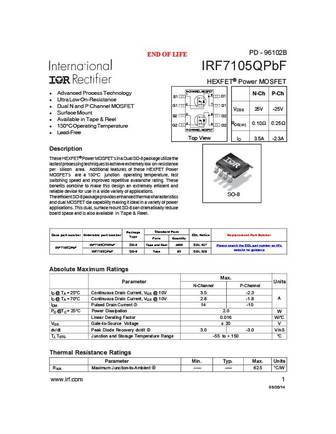
PD - 96102B END OF LIFE IRF7105QPbF HEXFET Power MOSFET N-CHANNEL MOSFET l Advanced Process Technology 1 8 N-Ch P-Ch S1 D1 l Ultra Low On-Resistance 2 7 G1 D1 l Dual N and P Channel MOSFET VDSS 25V -25V l Surface Mount 3 6 S2 D2 l Available in Tape & Reel 4 5 RDS(on) 0.10 0.25 G2 D2 l 150 C Operating Temperature P-CHANNEL MOSFET l Lead-Free Top View ID 3.5A -2.3A ... See More ⇒
9.4. Size:158K international rectifier
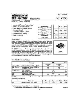
irf7106.pdf 

PD - 9.1098B IRF7106 PRELIMINARY HEXFET Power MOSFET Advanced Process Technology N-CHANNEL MOSFET Ultra Low On-Resistance N-Ch P-Ch 1 8 S1 D1 Dual N and P Channel Mosfet 2 7 G1 D1 Surface Mount VDSS 20V -20V 3 6 Available in Tape & Reel S2 D2 Dynamic dv/dt Rating RDS(on) 0.125 0.20 4 5 G2 D2 Fast Switching P-CHANNEL MOSFET ID 3.0A -2.5A Top View Description Four... See More ⇒
9.5. Size:158K international rectifier
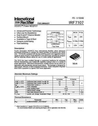
irf7107.pdf 

PD - 9.1099B IRF7107 PRELIMINARY HEXFET Power MOSFET Advanced Process Technology N-CHANNEL MOSFET N-Ch P-Ch Ultra Low On-Resistance 1 8 S1 D1 Dual N and P Channel Mosfet 2 7 G1 D1 VDSS 20V -20V Surface Mount 3 6 Available in Tape & Reel S2 D2 RDS(on) 0.125 0.160 Dynamic dv/dt Rating 4 5 G2 D2 Fast Switching P-CHANNEL MOSFET ID 3.0A -2.8A Top View Description F... See More ⇒
9.6. Size:609K international rectifier
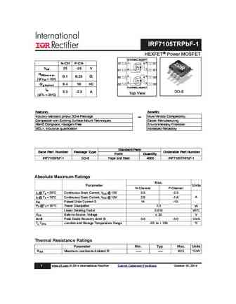
irf7105pbf-1.pdf 

IRF7105TRPbF-1 HEXFET Power MOSFET N-CHANNEL MOSFET 1 8 N-CH P-CH S1 D1 VDS 25 -25 V 2 7 G1 D1 RDS(on) max 3 6 0.1 0.25 S2 D2 (@V = 10V) GS 4 5 G2 D2 Qg (typical) 9.4 10 nC P-CHANNEL MOSFET ID 3.5 -2.3 A SO-8 Top View (@T = 25 C) A Features Benefits Industry-standard pinout SO-8 Package Multi-Vendor Compatibility Compatible with Existing Surface Mount Techn... See More ⇒
9.7. Size:304K international rectifier
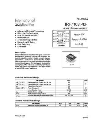
irf7103ipbf.pdf 

PD -96085A IRF7103IPbF HEXFET Power MOSFET l Adavanced Process Technology 1 8 l Ultra Low On-Resistance S1 D1 VDSS = 50V 2 7 l Dual N-Channel MOSFET G1 D1 l Surface Mount 3 6 S2 D2 RDS(on) = 0.130 l Available in Tape & Reel 4 5 G2 D2 l Dynamic dv/dt Rating ID = 3.0A l Fast Switching Top View l Lead-Free Description The SO-8 has been modified through a customized lea... See More ⇒
9.8. Size:303K international rectifier
irf7103pbf.pdf 

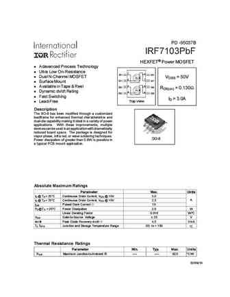
PD -95037B IRF7103PbF HEXFET Power MOSFET l Adavanced Process Technology l Ultra Low On-Resistance 1 8 S1 D1 l Dual N-Channel MOSFET VDSS = 50V 2 7 G1 D1 l Surface Mount 3 6 l Available in Tape & Reel S2 D2 RDS(on) = 0.130 l Dynamic dv/dt Rating 4 5 G2 D2 l Fast Switching ID = 3.0A Top View l Lead-Free Description The SO-8 has been modified through a customized leadf... See More ⇒
9.9. Size:1710K international rectifier
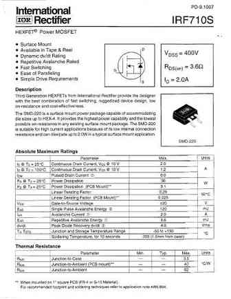
irf710spbf.pdf 

PD- 95746 IRF710SPbF Lead-Free 8/23/04 Document Number 91042 www.vishay.com 1 IRF710SPbF Document Number 91042 www.vishay.com 2 IRF710SPbF Document Number 91042 www.vishay.com 3 IRF710SPbF Document Number 91042 www.vishay.com 4 IRF710SPbF Document Number 91042 www.vishay.com 5 IRF710SPbF Document Number 91042 www.vishay.com 6 IRF710SPbF Peak Diode Recovery ... See More ⇒
9.10. Size:169K international rectifier
irf7103q.pdf 

PD - 93944C IRF7103Q AUTOMOTIVE MOSFET Typical Applications Anti-lock Braking Systems (ABS) HEXFET Power MOSFET Electronic Fuel Injection ) ) ) ) Power Doors, Windows & Seats VDSS RDS(on) max (m ) ID Benefits 50V 130@VGS = 10V 3.0A Advanced Process Technology 200@VGS = 4.5V 1.5A Dual N-Channel MOSFET Ultra Low On-Resistance 175 C Operating Temperature R... See More ⇒
9.11. Size:263K international rectifier
irf7101.pdf 

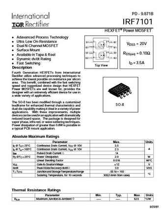
PD - 9.871B IRF7101 HEXFET Power MOSFET Adavanced Process Technology 1 8 Ultra Low On-Resistance D1 S1 VDSS = 20V Dual N-Channel MOSFET 2 7 G1 D1 Surface Mount 3 6 S2 D2 RDS(on) = 0.10 Available in Tape & Reel 4 5 G2 D2 Dynamic dv/dt Rating ID = 3.5A Fast Switching Top View Description Fourth Generation HEXFETs from International Rectifier utilize advanced pro... See More ⇒
9.12. Size:158K international rectifier
irf7104.pdf 

PD - 9.1096B IRF7104 HEXFET Power MOSFET Adavanced Process Technology 1 8 S1 D1 Ultra Low On-Resistance VDSS = -20V Dual P-Channel MOSFET 2 7 G1 D1 Surface Mount 3 6 S2 D2 RDS(on) = 0.250 Available in Tape & Reel 4 5 G2 D2 Dynamic dv/dt Rating ID = -2.3A Fast Switching Top View Description Fourth Generation HEXFETs from International Rectifier utilize advanced... See More ⇒
9.14. Size:275K international rectifier
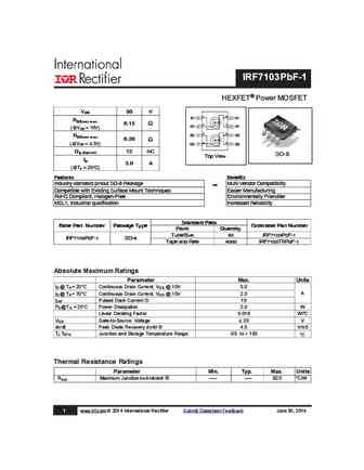
irf7103pbf-1.pdf 

IRF7103PbF-1 HEXFET Power MOSFET VDS 50 V 1 8 S1 D1 RDS(on) max 0.13 2 7 G1 D1 (@V = 10V) GS 3 6 S2 D2 RDS(on) max 0.20 4 5 (@V = 4.5V) G2 D2 GS Qg (typical) 12 nC SO-8 Top View ID 3.0 A (@T = 25 C) A Features Benefits Industry-standard pinout SO-8 Package Multi-Vendor Compatibility Compatible with Existing Surface Mount Techniques Easier Manufacturin... See More ⇒
9.15. Size:229K international rectifier
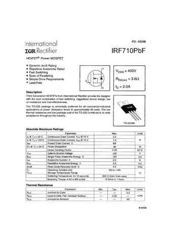
irf710pbf.pdf 

PD - 95366 IRF710PbF Lead-Free www.irf.com 1 6/10/04 IRF710PbF 2 www.irf.com IRF710PbF www.irf.com 3 IRF710PbF 4 www.irf.com IRF710PbF www.irf.com 5 IRF710PbF 6 www.irf.com IRF710PbF TO-220AB Package Outline Dimensions are shown in millimeters (inches) 10.54 (.415) - B - 3.78 (.149) 10.29 (.405) 2.87 (.113) 4.69 (.185) 3.54 (.139) 2.62 (.103) 4.20 (.165) - A - ... See More ⇒
9.16. Size:215K international rectifier
irf7104pbf.pdf 

PD - 95254 IRF7104PbF HEXFET Power MOSFET l Adavanced Process Technology l Ultra Low On-Resistance 1 8 S1 D1 l Dual P-Channel MOSFET VDSS = -20V 2 7 G1 D1 l Surface Mount l Available in Tape & Reel 3 6 S2 D2 RDS(on) = 0.250 l Dynamic dv/dt Rating 4 5 G2 D2 l Fast Switching ID = -2.3A l Lead-Free Top View Description Fourth Generation HEXFETs from International Recti... See More ⇒
9.17. Size:169K international rectifier
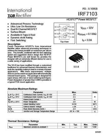
irf7103.pdf 

PD - 9.1095B IRF7103 HEXFET Power MOSFET Adavanced Process Technology 1 8 Ultra Low On-Resistance D1 S1 VDSS = 50V Dual N-Channel MOSFET 2 7 G1 D1 Surface Mount 3 6 S2 D2 RDS(on) = 0.130 Available in Tape & Reel 4 5 G2 D2 Dynamic dv/dt Rating ID = 3.0A Fast Switching Top View Description Fourth Generation HEXFETs from International Rectifier utilize advanced p... See More ⇒
9.18. Size:224K international rectifier
irf7105.pdf 

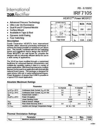
PD - 9.1097C IRF7105 HEXFET Power MOSFET Advanced Process Technology N-CHANNEL MOSFET 1 8 N-Ch P-Ch S1 D1 Ultra Low On-Resistance 2 7 Dual N and P Channel Mosfet G1 D1 VDSS 25V -25V Surface Mount 3 6 S2 D2 Available in Tape & Reel 4 5 RDS(on) 0.10 0.25 G2 D2 Dynamic dv/dt Rating P-CHANNEL MOSFET Fast Switching Top View ID 3.5A -2.3A Description Fourth Ge... See More ⇒
9.19. Size:302K international rectifier
irf7105pbf.pdf 

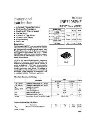
PD - 95164 IRF7105PbF HEXFET Power MOSFET l Advanced Process Technology l Ultra Low On-Resistance N-CHANNEL MOSFET 1 8 N-Ch P-Ch S1 D1 l Dual N and P Channel Mosfet 2 7 l Surface Mount G1 D1 VDSS 25V -25V l Available in Tape & Reel 3 6 S2 D2 l Dynamic dv/dt Rating 4 5 RDS(on) 0.10 0.25 G2 D2 l Fast Switching P-CHANNEL MOSFET l Lead-Free Top View ID 3.5A -2.3A ... See More ⇒
9.21. Size:275K international rectifier
irf7101pbf.pdf 

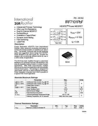
PD - 95162 IRF7101PbF HEXFET Power MOSFET l Adavanced Process Technology l Ultra Low On-Resistance 1 8 l Dual N-Channel MOSFET S1 D1 VDSS = 20V l Surface Mount 2 7 G1 D1 l Available in Tape & Reel 3 6 S2 D2 RDS(on) = 0.10 l Dynamic dv/dt Rating 4 5 G2 D2 l Fast Switching l Lead-Free ID = 3.5A Top View Description Fourth Generation HEXFETs from International Rectifi... See More ⇒
9.22. Size:743K international rectifier
irf7171m.pdf 

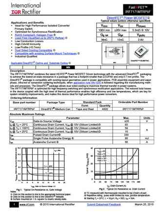
FastIRFET IRF7171MTRPbF DirectFET Power MOSFET Typical values (unless otherwise specified) Applications and Benefits Ideal for High Performance Isolated Converter VDSS VGS RDS(on) Primary Switch 100V min 20V max 5.3m @ 10V Optimized for Synchronous Rectification RoHS Compliant, Halogen Free Qg tot Qgd Vgs(th) Lead-Free (Qualified u... See More ⇒
9.23. Size:859K fairchild semi
irf710b.pdf 

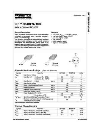
November 2001 IRF710B/IRFS710B 400V N-Channel MOSFET General Description Features These N-Channel enhancement mode power field effect 2.0A, 400V, RDS(on) = 3.4 @VGS = 10 V transistors are produced using Fairchild s proprietary, Low gate charge ( typical 7.7 nC) planar, DMOS technology. Low Crss ( typical 6.0 pF) This advanced technology has been especially tailored to ... See More ⇒
9.24. Size:209K samsung
irf710a.pdf 

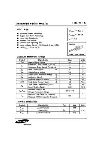
IRF710A Advanced Power MOSFET FEATURES BVDSS = 400 V Avalanche Rugged Technology RDS(on) = 3.6 Rugged Gate Oxide Technology Lower Input Capacitance ID = 2 A Improved Gate Charge Extended Safe Operating Area TO-220 Lower Leakage Current 10 A (Max.) @ VDS = 400V Low RDS(ON) 2.815 (Typ.) 1 2 3 1.Gate 2. Drain 3. Source Absolute Maximum Ratings Symbol Cha... See More ⇒
9.25. Size:198K vishay
irf710spbf sihf710s.pdf 

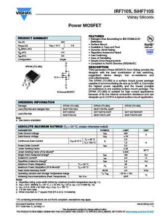
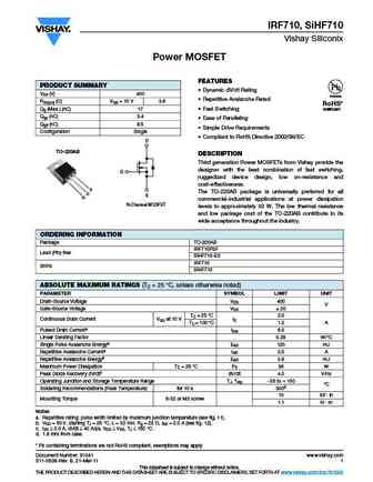
IRF710S, SiHF710S Vishay Siliconix Power MOSFET FEATURES PRODUCT SUMMARY Halogen-free According to IEC 61249-2-21 Definition VDS (V) 400 Surface Mount RDS(on) ( )VGS = 10 V 3.6 Available in Tape and Reel Qg (Max.) (nC) 17 Dynamic dV/dt Rating Qgs (nC) 3.4 Repetitive Avalanche Rated Fast Switching Qgd (nC) 8.5 Ease of Paralleling Configuration Sin... See More ⇒
9.26. Size:203K vishay
irf710 sihf710.pdf 

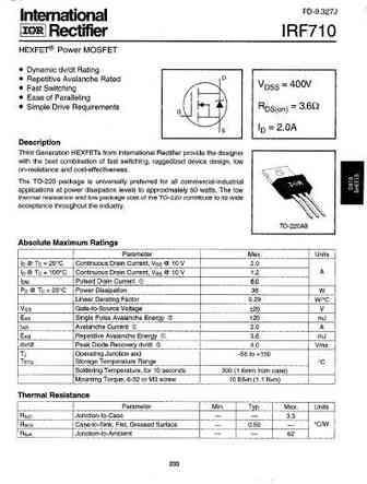
IRF710, SiHF710 Vishay Siliconix Power MOSFET FEATURES PRODUCT SUMMARY Dynamic dV/dt Rating VDS (V) 400 Available Repetitive Avalanche Rated RDS(on) ( )VGS = 10 V 3.6 RoHS* Qg (Max.) (nC) 17 Fast Switching COMPLIANT Qgs (nC) 3.4 Ease of Paralleling Qgd (nC) 8.5 Simple Drive Requirements Configuration Single Compliant to RoHS Directive 2002/95/EC D TO... See More ⇒
9.28. Size:899K cn vbsemi
irf7103tr.pdf 

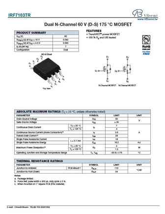
IRF7103TR www.VBsemi.tw Dual N-Channel 60 V (D-S) 175 C MOSFET FEATURES PRODUCT SUMMARY TrenchFET power MOSFET VDS (V) 60 100 % Rg and UIS tested RDS(on) ( ) at VGS = 10 V 0.040 RDS(on) ( ) at VGS = 4.5 V 0.055 ID (A) per leg 7 Configuration Dual SO-8 Dual D2 D1 D2 D2 5 D1 6 D1 7 8 G1 G2 4 G2 3 3 S1 S2 S2 S2 2 2 G G1 1 1 N-Channel MOSFET N-Channe... See More ⇒
9.29. Size:852K cn vbsemi
irf7101tr.pdf 

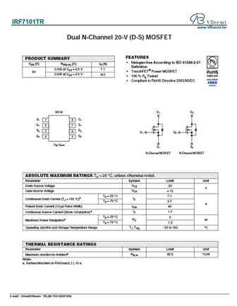
IRF7101TR www.VBsemi.tw Dual N-Channel 20-V (D-S) MOSFET FEATURES PRODUCT SUMMARY Halogen-free According to IEC 61249-2-21 VDS (V) RDS(on) ( )ID (A) Definition 0.025 at VGS = 4.5 V 7.1 TrenchFET Power MOSFET 20 0.035 at VGS = 2.5 V 6.0 100 % Rg Tested Compliant to RoHS Directive 2002/95/EC SO-8 D1 D2 S1 1 D1 8 G1 2 D1 7 S2 3 D2 6 G1 G2 G2 4 D2 5 ... See More ⇒
9.30. Size:1286K cn vbsemi
irf7105trpbf.pdf 

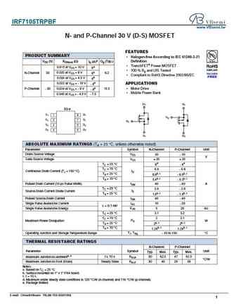
IRF7105TRPBF www.VBsemi.tw N- and P-Channel 30 V (D-S) MOSFET FEATURES PRODUCT SUMMARY Halogen-free According to IEC 61249-2-21 VDS (V) RDS(on) ( ) Definition ID (A)a Qg (Typ.) TrenchFET Power MOSFET 0.018 at VGS = 10 V 8e 100 % Rg and UIS Tested N-Channel 30 0.020 at VGS = 8 V 8e 6.2 Compliant to RoHS Directive 2002/95/EC 0.024 at VGS = 4.5 V 8e 0.032 at... See More ⇒
9.31. Size:234K inchange semiconductor
irf710.pdf 
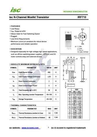
isc N-Channel Mosfet Transistor IRF710 FEATURES Low R DS(on) V Rated at 20V GS Silicon Gate for Fast Switching Speed Rugged Low Drive Requirements Minimum Lot-to-Lot variations for robust device performance and reliable operation DESCRITION Designed especially for high voltage,high speed applications, such as off-line switching power supplies , UPS,AC and DC mo... See More ⇒
Detailed specifications: IRF644S
, IRF645
, IRF646
, IRF650A
, IRF654A
, IRF710
, IRF710A
, IRF710S
, IRFZ48N
, IRF712
, IRF713
, IRF720
, IRF7201
, IRF7204
, IRF7205
, IRF7207
, IRF720A
.
Keywords - IRF711 MOSFET specs
IRF711 cross reference
IRF711 equivalent finder
IRF711 pdf lookup
IRF711 substitution
IRF711 replacement
Step-by-step guide to finding a MOSFET replacement. Cross-reference parts and ensure compatibility for your repair or project.
