All MOSFET. SI2312DS Datasheet


SI2312DS MOSFET. Datasheet pdf. Equivalent


   Type Designator: SI2312DS
   Marking Code: C2*
   Type of Transistor: MOSFET
   Type of Control Channel: N -Channel
   Pdⓘ - Maximum Power Dissipation: 1.25 W
   |Vds|ⓘ - Maximum Drain-Source Voltage: 20 V
   |Vgs|ⓘ - Maximum Gate-Source Voltage: 8 V
   |Vgs(th)|ⓘ - Maximum Gate-Threshold Voltage: 0.85 V
   |Id|ⓘ - Maximum Drain Current: 4.9 A
   Tjⓘ - Maximum Junction Temperature: 150 °C
   Qgⓘ - Total Gate Charge: 4.9 nC
   trⓘ - Rise Time: 40 nS
   Rdsⓘ - Maximum Drain-Source On-State Resistance: 0.027 Ohm
   Package: SOT23

 SI2312DS Transistor Equivalent Substitute - MOSFET Cross-Reference Search


SI2312DS Datasheet (PDF)

 ..1. Size:85K  vishay
si2312ds.pdf

SI2312DS SI2312DS

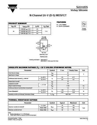
Si2312DSVishay SiliconixN-Channel 20 -V (D-S) MOSFETFEATURESPRODUCT SUMMARYD 1.8-V RatedD RoHS CompliantVDS (V) rDS(on) (W) ID (A) Qg (Typ)Pb-free0.033 @ VGS = 4.5 V 4.9Available0.040 @ VGS = 2.5 V 4.420 11.20.051 @ VGS = 1.8 V 3.9TO-236(SOT-23)G 13 DS 2Top ViewSi2312DS (C2)**Marking CodeOrdering Information: Si2312DS-T1Si2312DS-T1E3 (Lead (Pb)-F

 ..2. Size:1660K  kexin
si2312ds.pdf

SI2312DS SI2312DS

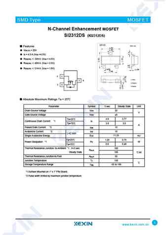
SMD Type MOSFETN-Channel Enhancement MOSFET SI2312DS (KI2312DS)SOT-23Unit: mm Features+0.12.9-0.1+0.10.4 -0.1 VDS (V) = 20V3 ID = 4.9 A (VGS =4.5V) RDS(ON) 33m (VGS = 4.5V) RDS(ON) 40m (VGS = 2.5V)1 2 RDS(ON) 51m (VGS = 1.8V) +0.1+0.050.95 -0.1 0.1 -0.011.9+0.1-0.1G 11.Gate3 D2.SourceS 23.Drain Abs

 ..3. Size:1476K  cn vbsemi
si2312ds.pdf

SI2312DS SI2312DS

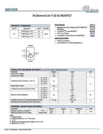
SI2312DSwww.VBsemi.twN-Channel 20 V (D-S) MOSFETFEATURESPRODUCT SUMMARY Halogen-free According to IEC 61249-2-21VDS (V) RDS(on) ()ID (A)e Qg (Typ.)Definition0.028 at VGS = 4.5 V TrenchFET Power MOSFET6a 100 % Rg Tested20 0.042 at VGS = 2.5 V 6a 8.8 nC Compliant to RoHS Directive 2002/95/EC0.050 at VGS = 1.8 V 5.6APPLICATIONS DC/DC Conve

 0.1. Size:1696K  kexin
si2312ds-3.pdf

SI2312DS SI2312DS

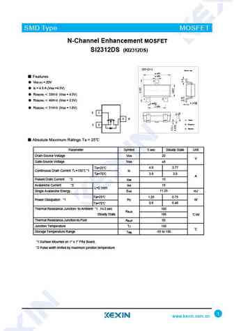
SMD Type MOSFETN-Channel Enhancement MOSFET SI2312DS (KI2312DS)SOT-23-3Unit: mm+0.22.9-0.1+0.10.4 -0.1 Features3 VDS (V) = 20V ID = 4.9 A (VGS =4.5V) RDS(ON) 33m (VGS = 4.5V)1 2 RDS(ON) 40m (VGS = 2.5V)+0.02+0.10.15 -0.020.95 -0.1+0.11.9 -0.2 RDS(ON) 51m (VGS = 1.8V)G 13 D1. Gate2. SourceS 23. Drain

 8.1. Size:126K  vishay
si2312cds.pdf

SI2312DS SI2312DS

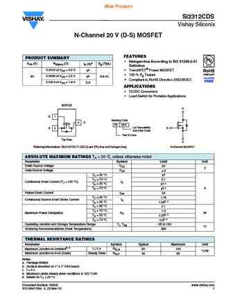
New ProductSi2312CDSVishay SiliconixN-Channel 20 V (D-S) MOSFETFEATURESPRODUCT SUMMARY Halogen-free According to IEC 61249-2-21VDS (V) RDS(on) ()ID (A)e Qg (Typ.)Definition0.0318 at VGS = 4.5 V TrenchFET Power MOSFET6a 100 % Rg Tested20 0.0356 at VGS = 2.5 V 6a 8.8 nC Compliant to RoHS Directive 2002/95/EC0.0414 at VGS = 1.8 V 5.6APPLI

 8.2. Size:213K  vishay
si2312bds.pdf

SI2312DS SI2312DS

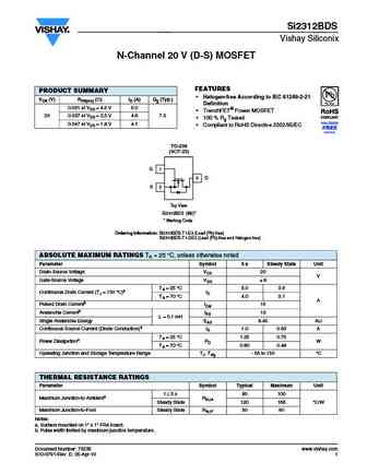
Si2312BDSVishay SiliconixN-Channel 20 V (D-S) MOSFETFEATURESPRODUCT SUMMARY Halogen-free According to IEC 61249-2-21VDS (V) RDS(on) ()ID (A) Qg (Typ.)Definition0.031 at VGS = 4.5 V 5.0 TrenchFET Power MOSFET20 0.037 at VGS = 2.5 V 4.6 7.5 100 % Rg Tested0.047 at VGS = 1.8 V 4.1 Compliant to RoHS Directive 2002/95/ECTO-236(SOT-23)G 13 DS 2

 8.3. Size:900K  mcc
si2312b.pdf

SI2312DS SI2312DS

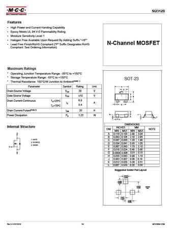
SI2312BFeatures High Power and Current Handing Capability Epoxy Meets UL 94 V-0 Flammability Rating Moisture Sensitivity Level 1 Halogen Free Available Upon Request By Adding Suffix "-HF"N-Channel MOSFET Lead Free Finish/RoHS Compliant ("P" Suffix Designates RoHS Compliant. See Ordering Information)Maximum RatingsOperating Junction Temperature Range: -55

 8.4. Size:1882K  htsemi
si2312.pdf

SI2312DS SI2312DS

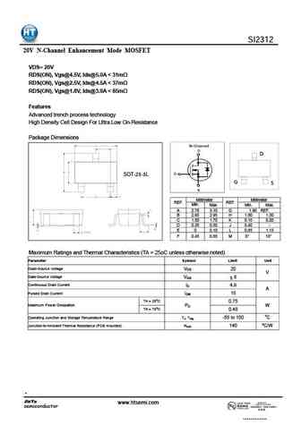
SI231220V N-Channel Enhancement Mode MOSFET VDS= 20V RDS(ON), Vgs@4.5V, Ids@5.0A

 8.5. Size:304K  shenzhen
si2312.pdf

SI2312DS SI2312DS

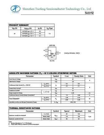
Shenzhen Tuofeng Semiconductor Technology Co., Ltd Si2312PRODUCT SUMMARYVDS (V) rDS(on) (W) ID (A) Qg (Typ)0.031 @ VGS = 4.5 V 5.00.037 @ VGS = 2.5 V 4.620 7.50.047 @ VGS = 1.8 V 4.1(SOT-23)G 13 DOrdering Information: Si2312S 2Top ViewABSOLUTE MAXIMUM RATINGS (TA = 25_C UNLESS OTHERWISE NOTED)Parameter Symbol 5 sec Steady State UnitDrain-Source Voltage VDS 20V

 8.6. Size:1794K  kexin
si2312 ki2312.pdf

SI2312DS SI2312DS

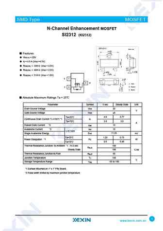
SMD Type MOSFETN-Channel Enhancement MOSFET SI2312 (KI2312)SOT-23-3Unit: mm+0.22.9-0.1+0.10.4 -0.1 Features3 VDS (V) = 20V ID = 4.9 A (VGS =4.5V) RDS(ON) 33m (VGS = 4.5V)1 2 RDS(ON) 40m (VGS = 2.5V)+0.02+0.10.15 -0.020.95 -0.1+0.11.9 -0.2 RDS(ON) 51m (VGS = 1.8V)G 13 D1. Gate2. SourceS 23. Drain Abs

 8.7. Size:1799K  umw-ic
si2312a.pdf

SI2312DS SI2312DS

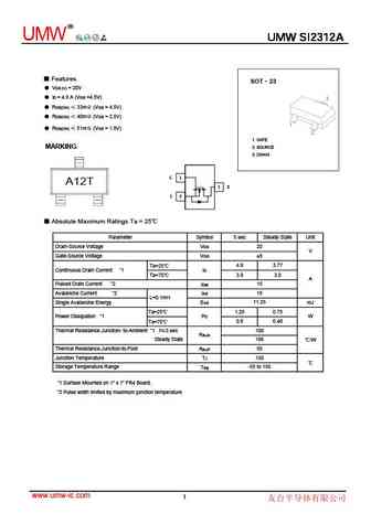
RUMWUMW SI2312AUMW SI2312A FeaturesSOT23 VDS (V) = 20V ID = 4.9 A (VGS =4.5V) RDS(ON) 33m (VGS = 4.5V) RDS(ON) 40m (VGS = 2.5V) RDS(ON) 51m (VGS = 1.8V)1. GATE MARKING 2. SOURCE 3. DRAIN G 1A12T3 DS 2 Absolute Maximum Ratings Ta = 25Parameter Symbol 5 sec Steady State Unit Drain-Source Voltage VDS 20V Gate

 8.8. Size:1164K  cn puolop
si2312.pdf

SI2312DS SI2312DS

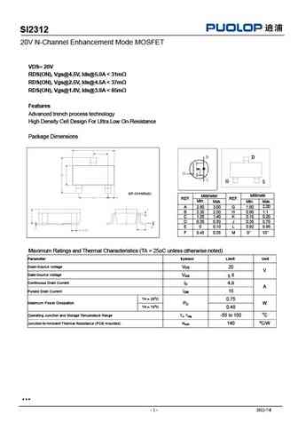
SI2312 20V N-Channel Enhancement Mode MOSFETVDS= 20V RDS(ON), Vgs@4.5V, Ids@5.0A

 8.9. Size:876K  cn vbsemi
si2312cds-t1-ge3.pdf

SI2312DS SI2312DS

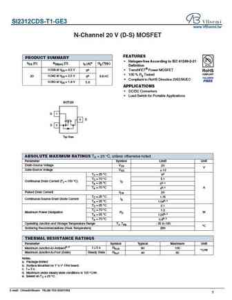
SI2312CDS-T1-GE3www.VBsemi.twN-Channel 20 V (D-S) MOSFETFEATURESPRODUCT SUMMARY Halogen-free According to IEC 61249-2-21VDS (V) RDS(on) ()ID (A)e Qg (Typ.)Definition0.028 at VGS = 4.5 V TrenchFET Power MOSFET6a 100 % Rg Tested20 0.042 at VGS = 2.5 V 6a 8.8 nC Compliant to RoHS Directive 2002/95/EC0.050 at VGS = 1.8 V 5.6APPLICATIONS DC/

 8.10. Size:907K  cn vbsemi
si2312bds-t1.pdf

SI2312DS SI2312DS

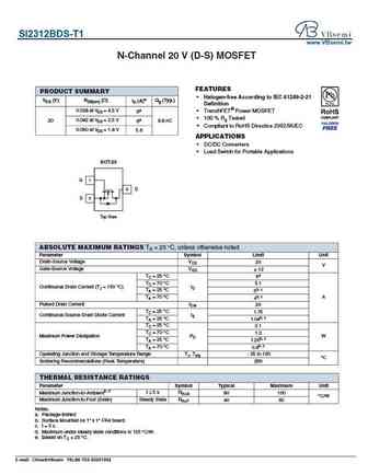
SI2312BDS-T1www.VBsemi.twN-Channel 20 V (D-S) MOSFETFEATURESPRODUCT SUMMARY Halogen-free According to IEC 61249-2-21VDS (V) RDS(on) ()ID (A)e Qg (Typ.)Definition0.028 at VGS = 4.5 V TrenchFET Power MOSFET6a 100 % Rg Tested20 0.042 at VGS = 2.5 V 6a 8.8 nC Compliant to RoHS Directive 2002/95/EC0.050 at VGS = 1.8 V 5.6APPLICATIONS DC/DC C

Datasheet: FMP36-015P , FMP76-01T , GMM3x100-01X1-SMD , FDMS0306AS , GMM3x120-0075X2-SMD , FDMS0300S , GMM3x160-0055X2-SMD , FDMC7200S , IRFB3607 , FDMC7200 , GMM3x60-015X2-SMD , FDMC0310AS , GWM100-0085X1-SL , FDMS3610S , GWM100-0085X1-SMD , FDMS3606S , GWM100-01X1-SL .


Back to Top