SM2315PSA Specs and Replacement
Type Designator: SM2315PSA
Type of Transistor: MOSFET
Type of Control Channel: P
-Channel
Absolute Maximum Ratings
Pd ⓘ
- Maximum Power Dissipation: 1.56
W
|Vds|ⓘ - Maximum Drain-Source Voltage: 30
V
|Vgs|ⓘ - Maximum Gate-Source Voltage: 20
V
|Id| ⓘ - Maximum Drain Current: 5
A
Tj ⓘ - Maximum Junction Temperature: 150
°C
Electrical Characteristics
tr ⓘ - Rise Time: 10
nS
Cossⓘ -
Output Capacitance: 105
pF
Rds ⓘ - Maximum Drain-Source On-State Resistance: 0.042
Ohm
Package:
SOT23
-
MOSFET ⓘ Cross-Reference Search
SM2315PSA datasheet
..1. Size:257K sino
sm2315psa.pdf 
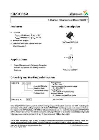
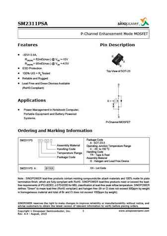
SM2315PSA P-Channel Enhancement Mode MOSFET Features Pin Description -30V/-5A, D RDS(ON) = 42m (max.) @ VGS =-10V S RDS(ON) = 64m (max.) @ VGS =-4.5V G Reliable and Rugged Top View of SOT-23-3 Lead Free and Green Devices Available (RoHS Compliant) D G Applications Power Management in Notebook Computer, S Portable Equipment and Battery Powered P-Channel MOSFET Systems... See More ⇒
9.2. Size:208K taiwansemi
tsm2311cx.pdf
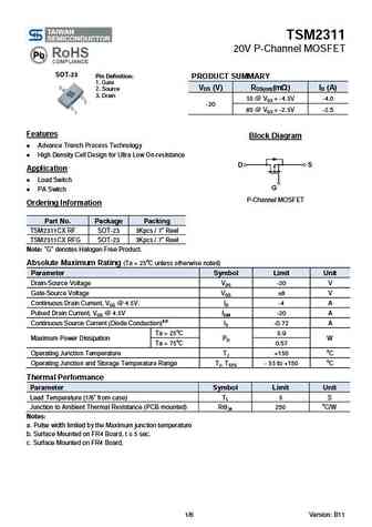
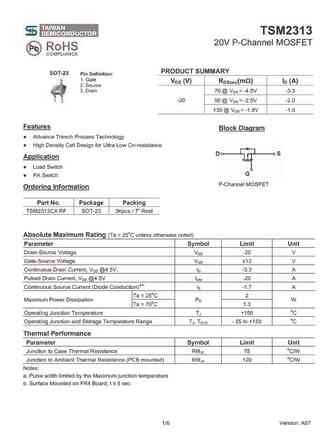
TSM2311 20V P-Channel MOSFET SOT-23 Pin Definition PRODUCT SUMMARY 1. Gate VDS (V) RDS(on)(m ) ID (A) 2. Source 3. Drain 55 @ VGS = -4.5V -4.0 -20 85 @ VGS = -2.5V -2.5 Features Block Diagram Advance Trench Process Technology High Density Cell Design for Ultra Low On-resistance Application Load Switch PA Switch P-Channel MOSFET Orderi... See More ⇒
9.3. Size:195K taiwansemi
tsm2314cx.pdf
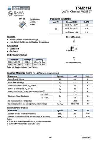
TSM2314 20V N-Channel MOSFET SOT-23 PRODUCT SUMMARY Pin Definition 1. Gate VDS (V) RDS(on)(m ) ID (A) 2. Source 3. Drain 33 @ VGS = 4.5V 4.9 40 @ VGS = 2.5V 4.4 20 100 @ VGS = 1.8V 2.9 Features Block Diagram Advance Trench Process Technology High Density Cell Design for Ultra Low On-resistance Application Load Switch PA Switch Orderin... See More ⇒
9.4. Size:239K taiwansemi
tsm2310cx.pdf
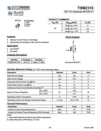
TSM2310 20V N-Channel MOSFET PRODUCT SUMMARY SOT-23 Pin Definition 1. Gate VDS (V) RDS(on)(m ) ID (A) 2. Source 33 @ VGS = 4.5V 4 3. Drain 20 40 @ VGS = 2.5V 3.2 100 @ VGS = 1.8V 2.0 Features Block Diagram Advance Trench Process Technology High Density Cell Design for Ultra Low On-resistance Application Load Switch PA Switch Ordering Info... See More ⇒
9.5. Size:213K taiwansemi
tsm2312cx.pdf
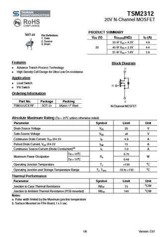
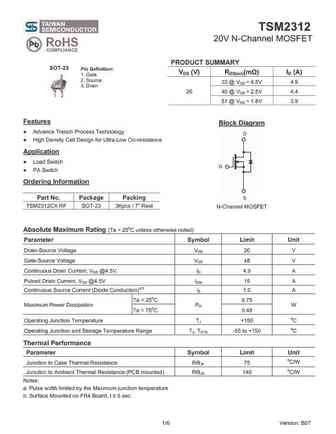
TSM2312 20V N-Channel MOSFET PRODUCT SUMMARY SOT-23 Pin Definition VDS (V) RDS(on)(m ) ID (A) 1. Gate 2. Source 33 @ VGS = 4.5V 4.9 3. Drain 20 40 @ VGS = 2.5V 4.4 51 @ VGS = 1.8V 3.9 Features Block Diagram Advance Trench Process Technology High Density Cell Design for Ultra Low On-resistance Application Load Switch PA Switch Ordering In... See More ⇒
9.8. Size:237K taiwansemi
tsm2318cx.pdf
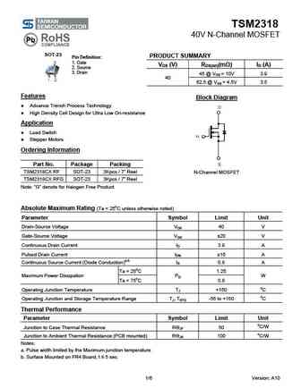
TSM2318 40V N-Channel MOSFET SOT-23 PRODUCT SUMMARY Pin Definition 1. Gate VDS (V) RDS(on)(m ) ID (A) 2. Source 3. Drain 45 @ VGS = 10V 3.9 40 62.5 @ VGS = 4.5V 3.5 Features Block Diagram Advance Trench Process Technology High Density Cell Design for Ultra Low On-resistance Application Load Switch Stepper Motors Ordering Information Pa... See More ⇒
9.9. Size:165K sino
sm2319psan.pdf

SM2319PSAN P-Channel Enhancement Mode MOSFET Features Pin Description -40V/-3A, D RDS(ON)= 80m (max.) @ VGS= -10V S RDS(ON)= 120m (max.) @ VGS= -4.5V G Reliable and Rugged Top View of SOT-23N Lead Free and Green Devices Available (RoHS Compliant) D Applications G Load Switch. DC/DC Converter. S P-Channel MOSFET Ordering and Marking Information Package ... See More ⇒
9.10. Size:259K sino
sm2317psa.pdf
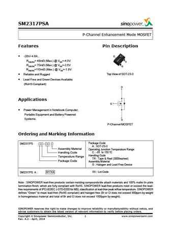
SM2317PSA P-Channel Enhancement Mode MOSFET Features Pin Description -20V/-4.6A , D RDS(ON)= 48m (Max.) @ VGS=-4.5V S RDS(ON)= 70m (Max.) @ VGS=-2.5V G RDS(ON)=110m (Max.) @ VGS=-1.8V Top View of SOT-23-3 Reliable and Rugged Lead Free and Green Devices Available (RoHS Compliant) D Applications G Power Management in Notebook Computer, Portable Equipment and Battery Powe... See More ⇒
9.11. Size:257K sino
sm2314nsa.pdf
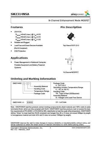
SM2314NSA N-Channel Enhancement Mode MOSFET Features Pin Description 20V/4.5A , D RDS(ON)=45m (max.) @ VGS=4.5V RDS(ON)=60m (max.) @ VGS=2.5V S RDS(ON)=85m (max.) @ VGS=1.8V G Reliable and Rugged Lead Free and Green Devices Available Top View of SOT-23-3 (RoHS Compliant) D ESD Protection Applications G Power Management in Notebook Computer, Portable Equipment and Batt... See More ⇒
9.12. Size:257K sino
sm2312nsa.pdf
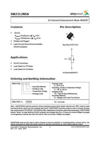
SM2312NSA N-Channel Enhancement Mode MOSFET Features Pin Description 30V/3A, D RDS(ON)=72m (max.) @ VGS=10V S RDS(ON)=100m (max.) @ VGS=4.5V G Reliable and Rugged Lead Free and Green Devices Available Top View of SOT-23-3 (RoHS Compliant) D Applications G DC-DC Conversion. Load Switch for PC fields. S Load Switch for Portables. N-Channel MOSFET Ordering and Marki... See More ⇒
9.13. Size:257K sino
sm2310nsa.pdf
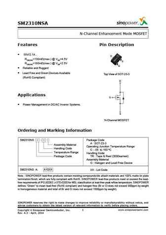
SM2310NSA N-Channel Enhancement Mode MOSFET Features Pin Description 55V/2.1A , D RDS(ON)=130m (max.) @ VGS=4.5V S RDS(ON)=180m (max.) @ VGS=2.5V G Reliable and Rugged Lead Free and Green Devices Available Top View of SOT-23-3 (RoHS Compliant) D Applications G Power Management in DC/AC Inverer Systems. S N-Channel MOSFET Ordering and Marking Information SM2310NS Pac... See More ⇒
9.14. Size:257K sino
sm2318nsa.pdf
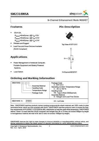
SM2318NSA N-Channel Enhancement Mode MOSFET Features Pin Description 30V/4.8A, D RDS(ON)=40m (max.) @ VGS=10V S RDS(ON)=48m (max.) @ VGS=4.5V G RDS(ON)=85m (max.) @ VGS=2.5V Reliable and Rugged Top View of SOT-23-3 Lead Free and Green Devices Available D (RoHS Compliant) Applications G Power Management in Notebook Computer, Portable Equipment and Battery Powered Sy... See More ⇒
9.15. Size:230K sino
sm2316nsa.pdf
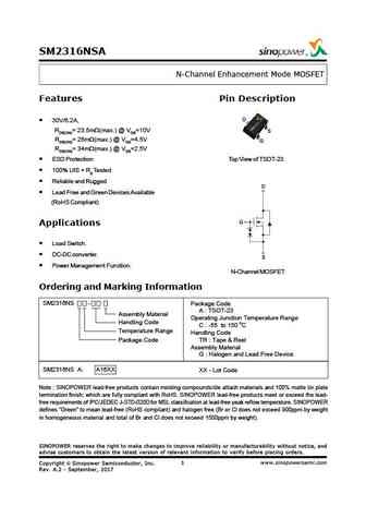
SM2316NSA N-Channel Enhancement Mode MOSFET Features Pin Description D 30V/6.2A, RDS(ON)= 23.5m (max.) @ VGS=10V S RDS(ON)= 26m (max.) @ VGS=4.5V G RDS(ON)= 34m (max.) @ VGS=2.5V ESD Protection Top View of TSOT-23 100% UIS + Rg Tested Reliable and Rugged D Lead Free and Green Devices Available (RoHS Compliant) G Applications Load Switch. DC-DC converter. S Po... See More ⇒
9.16. Size:165K sino
sm2311psa.pdf
SM2311PSA P-Channel Enhancement Mode MOSFET Features Pin Description -30V/-3.8A, D RDS(ON) = 62m (max.) @ VGS =-10V S RDS(ON) = 90m (max.) @ VGS =-4.5V G ESD Protection Top View of SOT-23 100% UIS + Rg Tested Reliable and Rugged Lead Free and Green Devices Available D (RoHS Compliant) Applications G Power Management in Notebook Computer, Portable Equipment and Ba... See More ⇒
9.17. Size:257K sino
sm2313psa.pdf

SM2313PSA P-Channel Enhancement Mode MOSFET Features Pin Description -20V/-3.5A, D RDS(ON)= 73m (Max.) @ VGS=-4.5V S RDS(ON)= 110m (Max.) @ VGS=-2.5V G RDS(ON)= 193m (Max.) @ VGS=-1.8V Top View of SOT-23-3 Reliable and Rugged Lead Free and Green Devices Available D (RoHS Compliant) G Applications Power Management in Notebook Computer, Portable Equipment and Battery Powe... See More ⇒
9.18. Size:944K globaltech semi
gsm2317.pdf
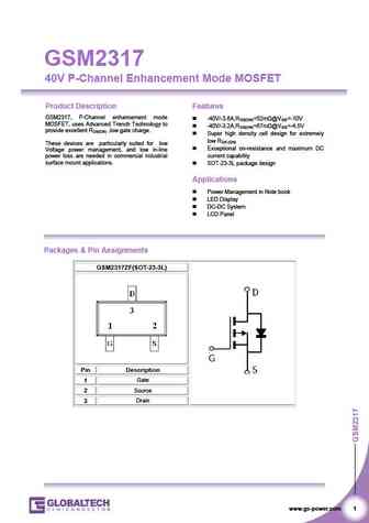
GSM2317 40V P-Channel Enhancement Mode MOSFET Product Description Features GSM2317, P-Channel enhancement mode -40V/-3.6A,RDS(ON)=52m @VGS=-10V MOSFET, uses Advanced Trench Technology to -40V/-3.2A,RDS(ON)=67m @VGS=-4.5V provide excellent RDS(ON) ,low gate charge. Super high density cell design for extremely low RDS (ON) These devices are particularly suited f... See More ⇒
9.19. Size:951K globaltech semi
gsm2319as.pdf
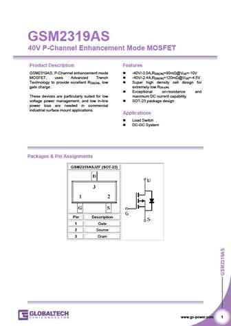
GSM2319AS 40V P-Channel Enhancement Mode MOSFET Product Description Features GSM2319AS, P-Channel enhancement mode -40V/-3.0A,RDS(ON)=90m @VGS=-10V MOSFET, uses Advanced Trench -40V/-2.4A,RDS(ON)=120m @VGS=-4.5V Technology to provide excellent RDS(ON), low Super high density cell design for gate charge. extremely low RDS (ON) Exceptional on-resistance and Thes... See More ⇒
9.20. Size:416K globaltech semi
gsm2311.pdf
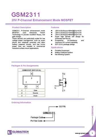
20V P-Channel Enhancement Mode MOSFET Product Description Features GSM2311, P-Channel enhancement mode -20V/-4.0A,RDS(ON)=56m @VGS=4.5V MOSFET, uses Advanced Trench -20V/-3.2A,RDS(ON)=70m @VGS=2.5V Technology to provide excellent RDS(ON), low -20V/-2.8A,RDS(ON)=96m @VGS=1.8V gate charge. Super high density cell design for These devices are particularly suited f... See More ⇒
9.21. Size:422K globaltech semi
gsm2318a.pdf
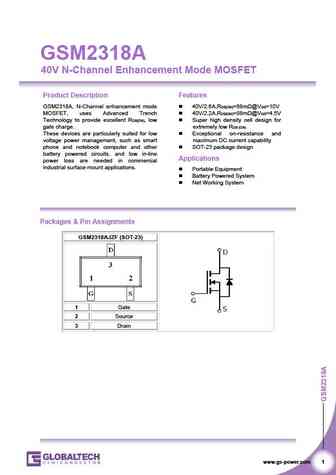
GSM2318A 40V N-Channel Enhancement Mode MOSFET Product Description Features GSM2318A, N-Channel enhancement mode 40V/2.6A,RDS(ON)=68m @VGS=10V MOSFET, uses Advanced Trench 40V/2.2A,RDS(ON)=88m @VGS=4.5V Technology to provide excellent RDS(ON), low Super high density cell design for gate charge. extremely low RDS (ON) These devices are particularly suited for low ... See More ⇒
9.22. Size:1189K globaltech semi
gsm2312.pdf
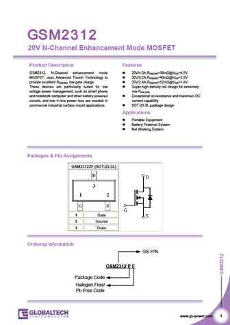
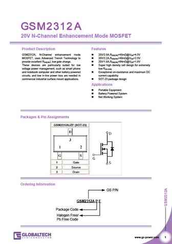
20V N-Channel Enhancement Mode MOSFET Product Description Features GSM2312, N-Channel enhancement mode 20V/4.0A,RDS(ON)=36m @VGS=4.5V MOSFET, uses Advanced Trench Technology to 20V/3.2A,RDS(ON)=40m @VGS=2.5V provide excellent RDS(ON), low gate charge. 20V/2.8A,RDS(ON)=52m @VGS=1.8V These devices are particularly suited for low Super high density cell design for e... See More ⇒
9.23. Size:461K globaltech semi
gsm2318.pdf
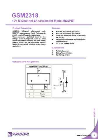
GSM2318 40V N-Channel Enhancement Mode MOSFET Product Description Features GSM2318, N-Channel enhancement mode 40V/3.6A,RDS(ON)=60m @VGS=10V MOSFET, uses Advanced Trench Technology to 40V/2.8A,RDS(ON)=80m @VGS=4.5V provide excellent RDS(ON) ,low gate charge. Super high density cell design for extremely These devices are particularly suited for low low RDS (ON) Volta... See More ⇒
9.24. Size:1024K globaltech semi
gsm2319a.pdf
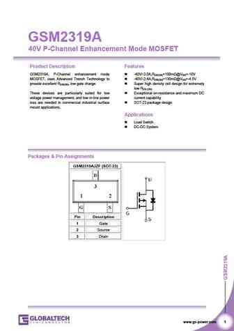
GSM2319A 40V P-Channel Enhancement Mode MOSFET Product Description Features GSM2319A, P-Channel enhancement mode -40V/-3.0A,RDS(ON)=100m @VGS=-10V MOSFET, uses Advanced Trench Technology to -40V/-2.4A,RDS(ON)=130m @VGS=-4.5V provide excellent RDS(ON), low gate charge. Super high density cell design for extremely low RDS (ON) These devices are particularly suited f... See More ⇒
9.25. Size:847K globaltech semi
gsm2311a.pdf
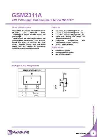
GSM2311A 20V P-Channel Enhancement Mode MOSFET Product Description Features GSM2311A, P-Channel enhancement mode -20V/-2.8A,RDS(ON)=68m @VGS=-4.5V MOSFET, uses Advanced Trench -20V/-2.2A,RDS(ON)=80m @VGS=-2.5V Technology to provide excellent RDS(ON), low -20V/-1.8A,RDS(ON)=105m @VGS=-1.8V gate charge. Super high density cell design for These devices are parti... See More ⇒
9.26. Size:1178K globaltech semi
gsm2312a.pdf
20V N-Channel Enhancement Mode MOSFET Product Description Features GSM2312A, N-Channel enhancement mode 20V/2.8A,RDS(ON)=45m @VGS=4.5V MOSFET, uses Advanced Trench Technology to 20V/2.2A,RDS(ON)=48m @VGS=2.5V provide excellent RDS(ON), low gate charge. 20V/1.8A,RDS(ON)=64m @VGS=1.8V These devices are particularly suited for low Super high density cell design for ... See More ⇒
9.27. Size:310K silicon standard
ssm2312gn.pdf

SSM2312GN N-channel Enhancement-mode Power MOSFET Low gate-charge BVDSS 20V D Simple drive requirement R 50m DS(ON) Fast switching ID 4.3A G Pb-free; RoHS compliant. S DESCRIPTION D The SSM2312GN is in a SOT-23-3 package, which is widely used for lower power commercial and industrial surface mount applications. This device is S suitable for low-voltage applications such as DC... See More ⇒
9.28. Size:313K silicon standard
ssm2313gn.pdf
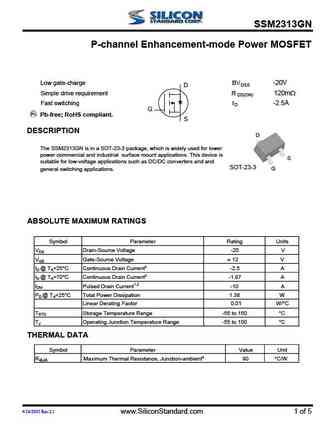
SSM2313GN P-channel Enhancement-mode Power MOSFET Low gate-charge BVDSS -20V D Simple drive requirement R 120m DS(ON) Fast switching ID -2.5A G Pb-free; RoHS compliant. S DESCRIPTION D The SSM2313GN is in a SOT-23-3 package, which is widely used for lower power commercial and industrial surface mount applications. This device is S suitable for low-voltage applications such as... See More ⇒
9.29. Size:498K silicon standard
ssm2316gn.pdf
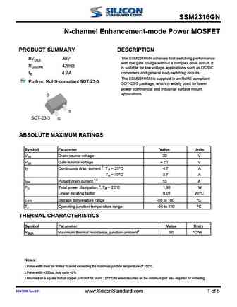
SSM2316GN N-channel Enhancement-mode Power MOSFET PRODUCT SUMMARY DESCRIPTION The SSM2316GN acheives fast switching performance BVDSS 30V with low gate charge without a complex drive circuit. It RDS(ON) 42m is suitable for low voltage applications such as DC/DC converters and general load-switching circuits. I 4.7A D The SSM2316GN is supplied in an RoHS-compliant Pb-free; RoHS-c... See More ⇒
9.30. Size:499K silicon standard
ssm2310gn.pdf
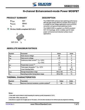
SSM2310GN N-channel Enhancement-mode Power MOSFET PRODUCT SUMMARY DESCRIPTION The SSM2310GN acheives fast switching performance BVDSS 60V with low gate charge without a complex drive circuit. It RDS(ON) 90m is suitable for low voltage applications such as DC/DC converters and general load-switching circuits. I 3A D The SSM2310GN is supplied in an RoHS-compliant Pb-free; RoHS-com... See More ⇒
9.31. Size:311K silicon standard
ssm2314gn.pdf

SSM2314GN N-channel Enhancement-mode Power MOSFET Low gate-charge BVDSS 20V D Simple drive requirement R 75m DS(ON) Fast switching ID 3.5A G Pb-free; RoHS compliant. S DESCRIPTION D The SSM2314GN is in a SOT-23-3 package, which is widely used for lower power commercial and industrial surface mount applications. This device is S suitable for low-voltage applications such as DC... See More ⇒
9.32. Size:497K silicon standard
ssm2318gen.pdf
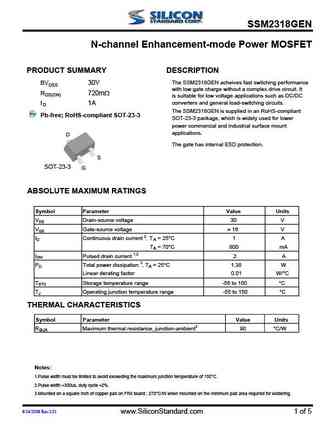
SSM2318GEN N-channel Enhancement-mode Power MOSFET PRODUCT SUMMARY DESCRIPTION The SSM2318GEN acheives fast switching performance BVDSS 30V with low gate charge without a complex drive circuit. It RDS(ON) 720m is suitable for low voltage applications such as DC/DC converters and general load-switching circuits. I 1A D The SSM2318GEN is supplied in an RoHS-compliant Pb-free; RoHS... See More ⇒
9.33. Size:769K cn sps
sm2312srl.pdf
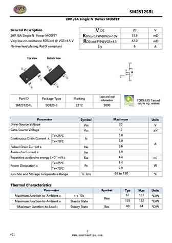
SM2312SRL 20V /6A Single N Power MOSFET B N02B N 20V /6A Single N Power MOSFET 6N02B General Description 20 V V DS 20V /6A Single N Power MOSFET 18.9 m RDS(on),TYP@VGS=10V Very low on-resistance RDS(on) @ VGS=4.5 V 42.0 m RDS(on),TYP@VGS=4.5 Pb-free lead plating; RoHS compliant 6 A ID Tape and reel Part ID Package Type Marking infomation 100% UIS Tested 100% Rg Tested SM231... See More ⇒
9.34. Size:3144K cn sps
sm2314.pdf
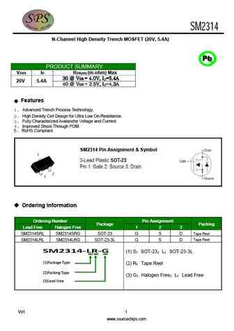
SM2314 N-Channel High Density Trench MOSFET (20V, 5.4A) Pb PRODUCT SUMMARY VDSS ID RDS(on) (m-ohm) Max 30 @ VGS = 4.0V, ID=5.4A 30 @ VGS = 4.0V, ID=5.4A 30 @ VGS = 4.0V, ID=5.4A 30 @ VGS = 4.0V, ID=5.4A 20V 5.4A 40 @ VGS = 2.5V, ID=4.3A 40 @ VGS = 2.5V, ID=4.3A 40 @ VGS = 2.5V, ID=4.3A 40 @ VGS = 2.5V, ID=4.3A Features 1 Advanced Trench Process Technology. ... See More ⇒
9.35. Size:912K cn vbsemi
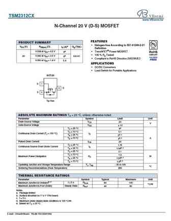
tsm2314cx.pdf

TSM2314CX www.VBsemi.tw N-Channel 20 V (D-S) MOSFET FEATURES PRODUCT SUMMARY Halogen-free According to IEC 61249-2-21 VDS (V) RDS(on) ( ) ID (A)e Qg (Typ.) Definition 0.028 at VGS = 4.5 V TrenchFET Power MOSFET 6a 100 % Rg Tested 20 0.042 at VGS = 2.5 V 6a 8.8 nC Compliant to RoHS Directive 2002/95/EC 0.050 at VGS = 1.8 V 5.6 APPLICATIONS DC/DC... See More ⇒
9.36. Size:911K cn vbsemi
tsm2312cx.pdf
TSM2312CX www.VBsemi.tw N-Channel 20 V (D-S) MOSFET FEATURES PRODUCT SUMMARY Halogen-free According to IEC 61249-2-21 VDS (V) RDS(on) ( ) ID (A)e Qg (Typ.) Definition 0.028 at VGS = 4.5 V TrenchFET Power MOSFET 6a 100 % Rg Tested 20 0.042 at VGS = 2.5 V 6a 8.8 nC Compliant to RoHS Directive 2002/95/EC 0.050 at VGS = 1.8 V 5.6 APPLICATIONS DC/DC... See More ⇒
9.37. Size:896K cn vbsemi
sm2312nsa.pdf
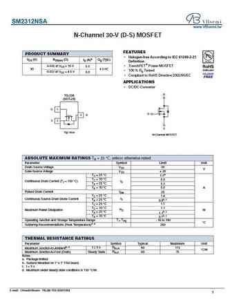
SM2312NSA www.VBsemi.tw N-Channel 30-V (D-S) MOSFET FEATURES PRODUCT SUMMARY Halogen-free According to IEC 61249-2-21 VDS (V) RDS(on) ( ) ID (A)a Qg (Typ.) Definition 0.030 at VGS = 10 V TrenchFET Power MOSFET 6.5 30 4.5 nC 100 % Rg Tested 0.033 at VGS = 4.5 V 6.0 Compliant to RoHS Directive 2002/95/EC APPLICATIONS DC/DC Converter D TO-236 (SOT-23) ... See More ⇒
Detailed specifications: SM4301PSU
, SM4301PSUC
, SM2303PSA
, SM2305PSA
, SM2307PSA
, SM2309PSA
, SM2311PSA
, SM2313PSA
, AON7408
, SM2317PSA
, SM2319PSAN
, SM2321PSA
, SM2323PSA
, SM2329PSA
, SM2331PSA
, SM2333PSA
, SM2335PSA
.
History: SM2305PSA
Keywords - SM2315PSA MOSFET specs
SM2315PSA cross reference
SM2315PSA equivalent finder
SM2315PSA pdf lookup
SM2315PSA substitution
SM2315PSA replacement
Need a MOSFET replacement?
Our guide shows you how to find a perfect substitute by comparing key parameters and specs