APM4568AK Specs and Replacement
Type Designator: APM4568AK
Type of Transistor: MOSFET
Type of Control Channel: NP-Channel
Absolute Maximum Ratings
Pd ⓘ
- Maximum Power Dissipation: 2 W
|Vds|ⓘ - Maximum Drain-Source Voltage: 40 V
|Vgs|ⓘ - Maximum Gate-Source Voltage: 16 V
|Id| ⓘ - Maximum Drain Current: 6.5(5) A
Tj ⓘ - Maximum Junction Temperature: 150 °C
Electrical Characteristics
Cossⓘ -
Output Capacitance: 120(130) pF
RDSonⓘ - Maximum Drain-Source On-State Resistance: 0.028(0.048) Ohm
Package: SOP8
- MOSFET ⓘ Cross-Reference Search
APM4568AK datasheet
..1. Size:225K anpec
apm4568ak.pdf 
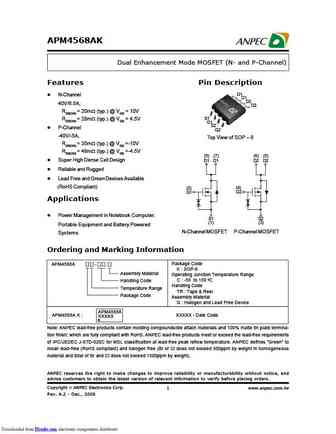
APM4568AK Dual Enhancement Mode MOSFET (N- and P-Channel) Features Pin Description D1 N-Channel D1 D2 40V/6.5A, D2 RDS(ON) = 20m (typ.) @ VGS = 10V S1 RDS(ON) = 28m (typ.) @ VGS = 4.5V G1 S2 P-Channel G2 -40V/-5A, Top View of SOP - 8 RDS(ON) = 35m (typ.) @ VGS =-10V RDS(ON) = 48m (typ.) @ VGS =-4.5V (8) (7) (6) (5) Super High Dense Cell Design D1 D1 D2 D2 ... See More ⇒
..2. Size:208K sino
apm4568ak.pdf
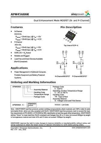
APM4568AK Dual Enhancement Mode MOSFET (N- and P-Channel) Features Pin Description D1 D1 N-Channel D2 D2 40V/6.5A, RDS(ON) = 20m (typ.) @ VGS = 10V S1 RDS(ON) = 28m (typ.) @ VGS = 4.5V G1 S2 G2 P-Channel -40V/-5A, Top View of SOP-8 RDS(ON) = 35m (typ.) @ VGS =-10V RDS(ON) = 48m (typ.) @ VGS =-4.5V (8) (7) (6) (5) 100% UIS + Rg Tested D1 D1 D2 D2 Reliabl... See More ⇒
7.1. Size:264K anpec
apm4568k.pdf
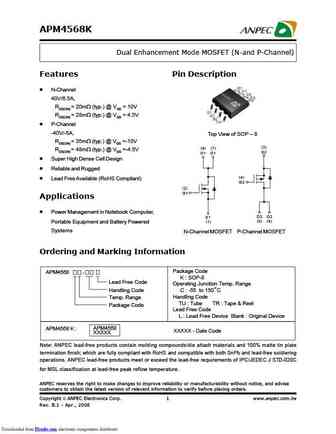
APM4568K Dual Enhancement Mode MOSFET (N-and P-Channel) Features Pin Description N-Channel 40V/6.5A, RDS(ON) = 20m (typ.) @ VGS = 10V RDS(ON) = 28m (typ.) @ VGS = 4.5V P-Channel -40V/-5A, Top View of SOP - 8 RDS(ON) = 35m (typ.) @ VGS =-10V (3) (8) (7) RDS(ON) = 48m (typ.) @ VGS =-4.5V S2 D1 D1 Super High Dense Cell Design Reliable and Rugged (4) Lead Free Av... See More ⇒
7.2. Size:224K anpec
apm4568j.pdf
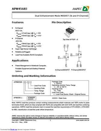
APM4568J Dual Enhancement Mode MOSFET (N-and P-Channel) Features Pin Description N-Channel 40V/7.5A, RDS(ON) =21m (typ.) @ VGS = 10V RDS(ON) =30m (typ.) @ VGS = 4.5V P-Channel Top View of PDIP - 8 -40V/-6A, RDS(ON) =36m (typ.) @ VGS =-10V (8) (7) (3) RDS(ON) =50m (typ.) @ VGS =-4.5V D1 D1 S2 Super High Dense Cell Design Reliable and Rugged (4) Lead Free Availab... See More ⇒
9.1. Size:241K anpec
apm4550j.pdf
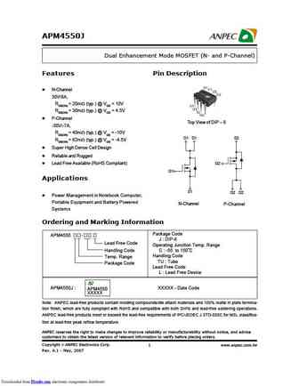
APM4550J Dual Enhancement Mode MOSFET (N- and P-Channel) Features Pin Description N-Channel 30V/8A, RDS(ON) = 20m (typ.) @ VGS = 10V RDS(ON) = 30m (typ.) @ VGS = 4.5V P-Channel Top View of DIP - 8 -30V/-7A, RDS(ON) = 40m (typ.) @ VGS = -10V D1 D1 S2 RDS(ON) = 62m (typ.) @ VGS = -4.5V Super High Dense Cell Design Reliable and Rugged Lead Free Available (RoHS Compl... See More ⇒
9.2. Size:265K anpec
apm4552k.pdf

APM4552K Dual Enhancement Mode MOSFET (N- and P-Channel) Features Pin Description D1 N-Channel D1 D2 30V/7A, D2 RDS(ON) = 23m (typ.) @ VGS = 10V RDS(ON) = 34m (typ.) @ VGS = 4.5V S1 P-Channel G1 -30V/-5A, S2 G2 RDS(ON) = 46m (typ.) @ VGS =-10V RDS(ON) = 62m (typ.) @ VGS =-4.5V Top View of SOP - 8 Super High Dense Cell Design (6) (5) (8) (7) D2 D2 D1 D1 ... See More ⇒
9.3. Size:180K anpec
apm4536k.pdf
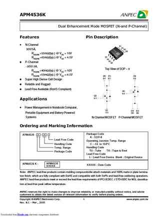
APM4536K Dual Enhancement Mode MOSFET (N-and P-Channel) Features Pin Description N-Channel D1 D1 30V/5A, D2 D2 RDS(ON) =35m (typ.) @ VGS = 10V S1 RDS(ON) =45m (typ.) @ VGS = 4.5V G1 S2 P-Channel G2 -30V/-5A, Top View of SOP - 8 RDS(ON) =40m (typ.) @ VGS =-10V RDS(ON) =55m (typ.) @ VGS =-4.5V (8) (7) (3) D1 D1 S2 Super High Dense Cell ... See More ⇒
9.4. Size:234K anpec
apm4532.pdf
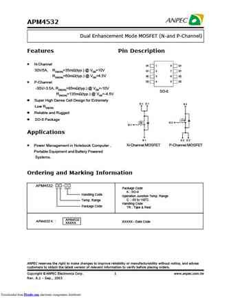
APM4532 Dual Enhancement Mode MOSFET (N-and P-Channel) Features Pin Description N-Channel S1 1 8 D1 30V/5A, RDS(ON)=35m (typ.) @ VGS=10V G1 2 7 D1 RDS(ON)=60m (typ.) @ VGS=4.5V S2 3 6 D2 G2 4 5 D2 P-Channel -30V/-3.5A, RDS(ON)=85m (typ.) @ VGS=-10V SO-8 RDS(ON)=135m (typ.) @ VGS=-4.5V Super High Dense Cell Design for Extremely D1 D1 S2 Lo... See More ⇒
9.5. Size:271K anpec
apm4534k.pdf
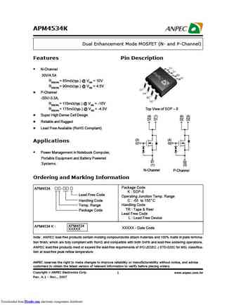
APM4534K Dual Enhancement Mode MOSFET (N- and P-Channel) Features Pin Description N-Channel 30V/4.5A RDS(ON) = 65m (typ.) @ VGS = 10V RDS(ON) = 90m (typ.) @ VGS = 4.5V P-Channel -30V/-3.3A, RDS(ON) = 110m (typ.) @ VGS = -10V RDS(ON) = 175m (typ.) @ VGS = -4.5V Top View of SOP - 8 Super High Dense Cell Design (8) (7) (6) (5) D1 D1 D2 D2 Reliable and Rugged Lea... See More ⇒
9.6. Size:263K anpec
apm4550k.pdf
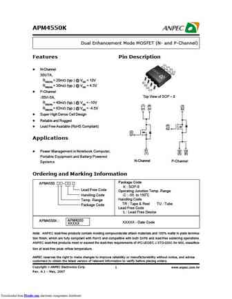
APM4550K Dual Enhancement Mode MOSFET (N- and P-Channel) Features Pin Description N-Channel 30V/7A, RDS(ON) = 20m (typ.) @ VGS = 10V RDS(ON) = 30m (typ.) @ VGS = 4.5V P-Channel Top View of SOP - 8 -30V/-5A, RDS(ON) = 40m (typ.) @ VGS = -10V (7) (8) (3) RDS(ON) = 62m (typ.) @ VGS = -4.5V D1 D1 S2 Super High Dense Cell Design Reliable and Rugged (4) Lead Free Av... See More ⇒
9.7. Size:342K anpec
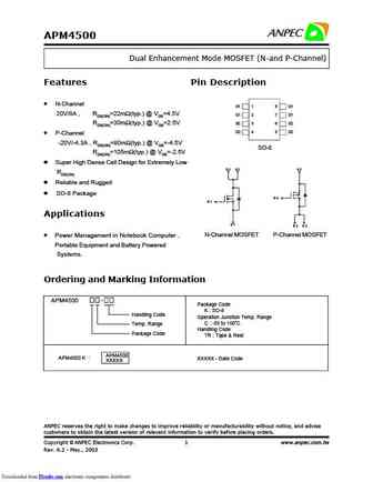
apm4500.pdf
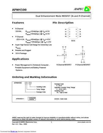
APM4500 Dual Enhancement Mode MOSFET (N-and P-Channel) Features Pin Description N-Channel S1 1 8 D1 20V/8A , RDS(ON)=22m (typ.) @ VGS=4.5V G1 2 7 D1 RDS(ON)=30m (typ.) @ VGS=2.5V S2 3 6 D2 G2 4 5 D2 P-Channel -20V/-4.3A , RDS(ON)=80m (typ.) @ VGS=-4.5V SO-8 RDS(ON)=105m (typ.) @ VGS=-2.5V Super High Dense Cell Design for Extremely Low D1 D1... See More ⇒
9.8. Size:240K anpec
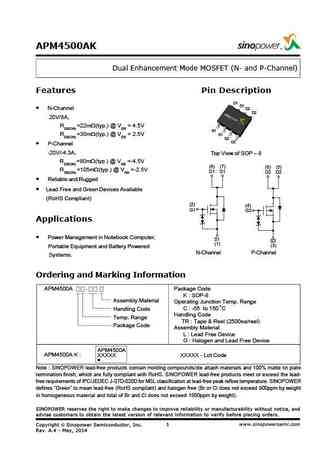
apm4500ak.pdf
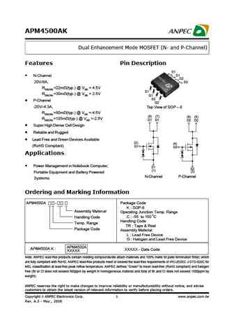
APM4500AK Dual Enhancement Mode MOSFET (N- and P-Channel) Features Pin Description D1 D1 N-Channel D2 D2 20V/8A, RDS(ON) =22m (typ.) @ VGS = 4.5V S1 RDS(ON) =30m (typ.) @ VGS = 2.5V G1 S2 P-Channel G2 -20V/-4.3A, Top View of SOP - 8 RDS(ON) =80m (typ.) @ VGS =-4.5V (8) (7) (6) (5) RDS(ON) =105m (typ.) @ VGS =-2.5V D1 D1 D2 D2 Super High Dense Cell Des... See More ⇒
9.9. Size:187K anpec
apm4532k.pdf

APM4532K Dual Enhancement Mode MOSFET (N-and P-Channel) Features Pin Description N-Channel D1 D1 D2 30V/5A, D2 RDS(ON) =35m (typ.) @ VGS = 10V S1 RDS(ON) =60m (typ.) @ VGS = 4.5V G1 S2 G2 P-Channel -30V/-3.5A, Top View of SOP - 8 RDS(ON) =85m (typ.) @ VGS =-10V (8) (7) (3) RDS(ON) =135m (typ.) @ VGS =-4.5V D1 D1 S2 Super High Dense C... See More ⇒
9.10. Size:198K anpec
apm4538k.pdf

APM4538K Dual Enhancement Mode MOSFET (N-and P-Channel) Features Pin Description N-Channel D1 D1 D2 36V/5A, D2 RDS(ON) =50m (typ.) @ VGS = 10V S1 RDS(ON) =60m (typ.) @ VGS = 4.5V G1 S2 G2 P-Channel -36V/-4A, Top View of SOP - 8 RDS(ON) =60m (typ.) @ VGS =-10V (3) RDS(ON) =80m (typ.) @ VGS =-4.5V (8) (7) S2 D1 D1 Super High Dense Cel... See More ⇒
9.11. Size:269K anpec
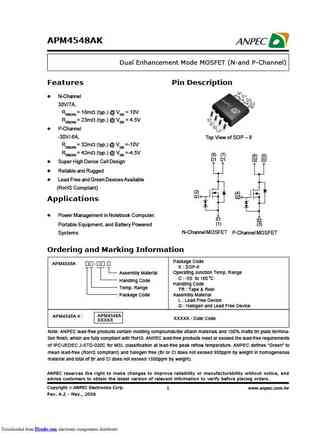
apm4548k.pdf
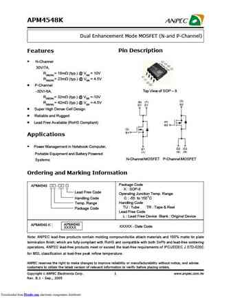
APM4548K Dual Enhancement Mode MOSFET (N-and P-Channel) Features Pin Description N-Channel 30V/7A, RDS(ON) = 18m (typ.) @ VGS = 10V RDS(ON) = 23m (typ.) @ VGS = 4.5V P-Channel Top View of SOP - 8 -30V/-6A, RDS(ON) = 32m (typ.) @ VGS =-10V (3) (8) (7) RDS(ON) = 42m (typ.) @ VGS =-4.5V S2 D1 D1 Super High Dense Cell Design Reliable and Rugged (4) Lead ... See More ⇒
9.12. Size:181K anpec
apm4542k.pdf

APM4542K Dual Enhancement Mode MOSFET (N-and P-Channel) Features Pin Description N-Channel D1 D1 D2 30V/7A, D2 RDS(ON) =17m (typ.) @ VGS = 10V S1 RDS(ON) =22m (typ.) @ VGS = 4.5V G1 S2 G2 P-Channel Top View of SOP - 8 -30V/-5.5A, RDS(ON) =35m (typ.) @ VGS =-10V (3) (8) (7) RDS(ON) =51m (typ.) @ VGS =-4.5V S2 D1 D1 Super High Dense C... See More ⇒
9.13. Size:703K anpec
apm4500k.pdf
APM4500 Dual Enhancement Mode MOSFET (N-and P-Channel) Features Pin Description N-Channel S1 1 8 D1 20V/8A , RDS(ON)=22m (typ.) @ VGS=4.5V G1 2 7 D1 RDS(ON)=30m (typ.) @ VGS=2.5V S2 3 6 D2 G2 4 5 D2 P-Channel -20V/-4.3A , RDS(ON)=80m (typ.) @ VGS=-4.5V SO-8 RDS(ON)=105m (typ.) @ VGS=-2.5V Super High Dense Cell Design for Extremely Low D1 D1... See More ⇒
9.14. Size:264K anpec
apm4548ak.pdf
APM4548AK Dual Enhancement Mode MOSFET (N-and P-Channel) Features Pin Description N-Channel 30V/7A, RDS(ON) = 18m (typ.) @ VGS = 10V RDS(ON) = 23m (typ.) @ VGS = 4.5V P-Channel -30V/-6A, Top View of SOP - 8 RDS(ON) = 32m (typ.) @ VGS =-10V RDS(ON) = 42m (typ.) @ VGS =-4.5V (8) (7) (6) (5) D1 D1 D2 D2 Super High Dense Cell Design Reliable and Rugged Lead Free a... See More ⇒
9.15. Size:265K anpec
apm4588k.pdf
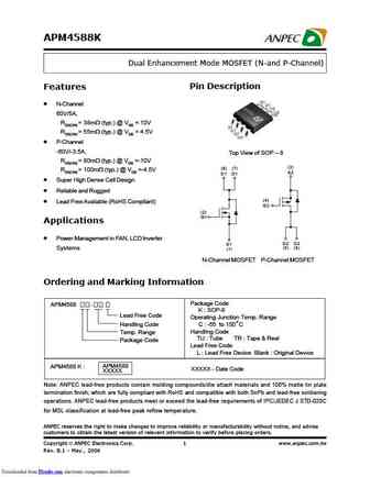
APM4588K Dual Enhancement Mode MOSFET (N-and P-Channel) Features Pin Description N-Channel 60V/5A, RDS(ON) = 38m (typ.) @ VGS = 10V RDS(ON) = 55m (typ.) @ VGS = 4.5V P-Channel -60V/-3.5A, Top View of SOP - 8 RDS(ON) = 80m (typ.) @ VGS =-10V (3) (8) (7) RDS(ON) = 100m (typ.) @ VGS =-4.5V S2 D1 D1 Super High Dense Cell Design Reliable and Rugged (4) Lead Free A... See More ⇒
9.16. Size:302K sino
apm4500ak.pdf
APM4500AK Dual Enhancement Mode MOSFET (N- and P-Channel) Features Pin Description D1 D1 N-Channel D2 D2 20V/8A, RDS(ON) =22m (typ.) @ VGS = 4.5V S1 RDS(ON) =30m (typ.) @ VGS = 2.5V G1 S2 G2 P-Channel -20V/-4.3A, Top View of SOP 8 RDS(ON) =80m (typ.) @ VGS =-4.5V (8) (7) (6) (5) RDS(ON) =105m (typ.) @ VGS =-2.5V D1 D1 D2 D2 Reliable and Rugged Lead Free and Gr... See More ⇒
9.17. Size:1667K cn vbsemi
apm4532kc.pdf
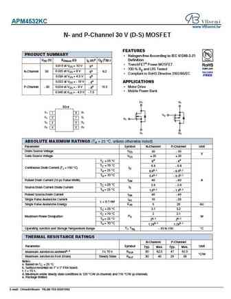
APM4532KC www.VBsemi.tw N- and P-Channel 30 V (D-S) MOSFET FEATURES PRODUCT SUMMARY Halogen-free According to IEC 61249-2-21 VDS (V) RDS(on) ( ) Definition ID (A)a Qg (Typ.) TrenchFET Power MOSFET 0.018 at VGS = 10 V 8e 100 % Rg and UIS Tested N-Channel 30 0.020 at VGS = 8 V 8e 6.2 Compliant to RoHS Directive 2002/95/EC 0.024 at VGS = 4.5 V 8e 0.032 at VG... See More ⇒
9.18. Size:1612K cn vbsemi
apm4550kc.pdf

APM4550KC www.VBsemi.tw N- and P-Channel 30 V (D-S) MOSFET FEATURES PRODUCT SUMMARY Halogen-free According to IEC 61249-2-21 VDS (V) RDS(on) ( ) Definition ID (A)a Qg (Typ.) TrenchFET Power MOSFET 0.018 at VGS = 10 V 8e 100 % Rg and UIS Tested N-Channel 30 0.020 at VGS = 8 V 8e 6.2 Compliant to RoHS Directive 2002/95/EC 0.024 at VGS = 4.5 V 8e 0.032 at VG... See More ⇒
Detailed specifications: SM3335PSQA, SM3335PSQG, SM3040CSU4, SM6042CSU4, SM1A40CSK, SM2001CSK, APM4500AK, APM2701AC, IRFZ48N, APM9938K, SM1620CSCS, SM1A40CSQ, SM1A42CSK, SM2221CSQG, SM2222CSQG, SM2607CSC, SM2620CSC
Keywords - APM4568AK MOSFET specs
APM4568AK cross reference
APM4568AK equivalent finder
APM4568AK pdf lookup
APM4568AK substitution
APM4568AK replacement
Step-by-step guide to finding a MOSFET replacement. Cross-reference parts and ensure compatibility for your repair or project.
