AOW292 Specs and Replacement
Type Designator: AOW292
Type of Transistor: MOSFET
Type of Control Channel: N-Channel
Absolute Maximum Ratings
Pd ⓘ
- Maximum Power Dissipation: 300 W
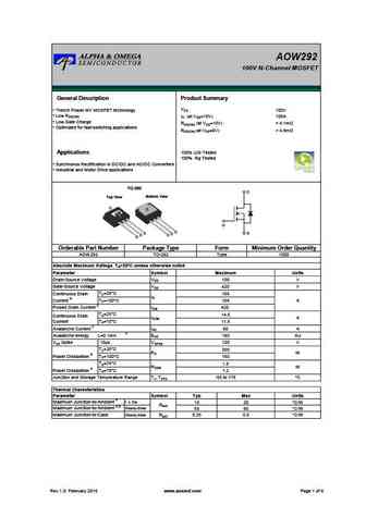
|Vds|ⓘ - Maximum Drain-Source Voltage: 100 V
|Vgs|ⓘ - Maximum Gate-Source Voltage: 20 V
|Id| ⓘ - Maximum Drain Current: 105 A
Tj ⓘ - Maximum Junction Temperature: 175 °C
Electrical Characteristics
tr ⓘ - Rise Time: 50 nS
Cossⓘ -
Output Capacitance: 557 pF
Rds ⓘ - Maximum Drain-Source On-State Resistance: 0.0041 Ohm
Package: TO262
- MOSFET ⓘ Cross-Reference Search
AOW292 datasheet
..2. Size:283K inchange semiconductor
aow292.pdf 

isc N-Channel MOSFET Transistor AOW292 FEATURES Drain Current I = 105A@ T =25 D C Drain Source Voltage- V = 100V(Min) DSS Static Drain-Source On-Resistance R = 4.7m (Max) DS(on) 100% avalanche tested Minimum Lot-to-Lot variations for robust device performance and reliable operation DESCRITION Be suitable for synchronous rectification for server and gene... See More ⇒
9.1. Size:251K aosemi
aow298.pdf
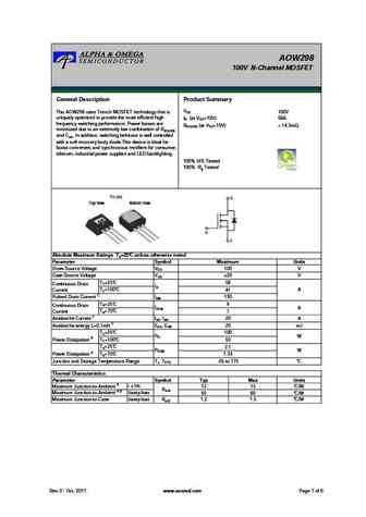
AOW298 100V N-Channel MOSFET General Description Product Summary VDS The AOW298 uses Trench MOSFET technology that is 100V uniquely optimized to provide the most efficient high ID (at VGS=10V) 58A frequency switching performance. Power losses are RDS(ON) (at VGS=10V) ... See More ⇒
9.2. Size:424K aosemi
aow296.pdf
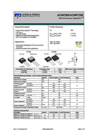
AOW296/AOWF296 TM 100V N-Channel AlphaSGT General Description Product Summary VDS 100V Trench Power AlphaSGTTM technology Low RDS(ON) RDS(ON) (at VGS=10V) ... See More ⇒
9.3. Size:253K aosemi
aow2918.pdf
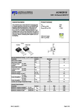
AOW2918 100V N-Channel MOSFET General Description Product Summary VDS The AOW2918 uses Trench MOSFET technology that 100V is uniquely optimized to provide the most efficient high ID (at VGS=10V) 90A frequency switching performance. Power losses are RDS(ON) (at VGS=10V) ... See More ⇒
9.4. Size:251K aosemi
aow29s50.pdf
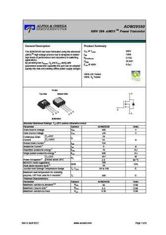
AOW29S50 TM 500V 29A MOS Power Transistor General Description Product Summary VDS @ Tj,max 600V The AOW29S50 has been fabricated using the advanced MOSTM high voltage process that is designed to deliver IDM 120A high levels of performance and robustness in switching RDS(ON),max 0.15 applications. Qg,typ 26.6nC By providing low RDS(on), Qg and EOSS along with ... See More ⇒
9.5. Size:310K aosemi
aow290.pdf
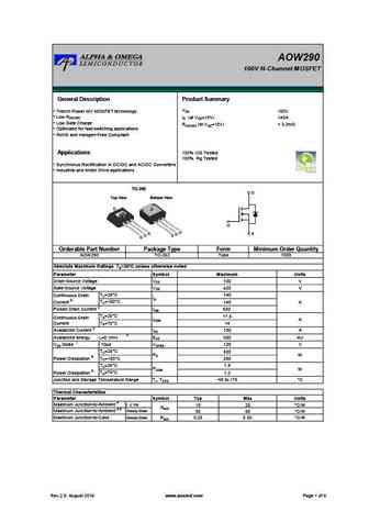
AOW290 100V N-Channel MOSFET General Description Product Summary VDS Trench Power MV MOSFET technology 100V Low RDS(ON) ID (at VGS=10V) 140A Low Gate Charge RDS(ON) (at VGS=10V) ... See More ⇒
9.6. Size:283K inchange semiconductor
aow298.pdf

isc N-Channel MOSFET Transistor AOW298 FEATURES Drain Current I = 58A@ T =25 D C Drain Source Voltage- V = 100V(Min) DSS Static Drain-Source On-Resistance R = 14.5m (Max) DS(on) 100% avalanche tested Minimum Lot-to-Lot variations for robust device performance and reliable operation DESCRITION Be suitable for synchronous rectification for server and gene... See More ⇒
9.7. Size:284K inchange semiconductor
aow296.pdf
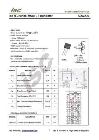
isc N-Channel MOSFET Transistor AOW296 FEATURES Drain Current I = 70A@ T =25 D C Drain Source Voltage- V = 100V(Min) DSS Static Drain-Source On-Resistance R = 9.7m (Max) DS(on) 100% avalanche tested Minimum Lot-to-Lot variations for robust device performance and reliable operation DESCRITION Be suitable for synchronous rectification for server and gener... See More ⇒
9.8. Size:283K inchange semiconductor
aow2918.pdf

isc N-Channel MOSFET Transistor AOW2918 FEATURES Drain Current I = 90A@ T =25 D C Drain Source Voltage- V = 100V(Min) DSS Static Drain-Source On-Resistance R = 7m (Max) DS(on) 100% avalanche tested Minimum Lot-to-Lot variations for robust device performance and reliable operation DESCRITION Be suitable for synchronous rectification for server and genera... See More ⇒
9.9. Size:300K inchange semiconductor
aow29s50.pdf
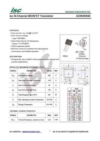
isc N-Channel MOSFET Transistor AOW29S50 FEATURES Drain Current I = 29A@ T =25 D C Drain Source Voltage- V = 500V(Min) DSS Static Drain-Source On-Resistance R = 0.15 (Max) DS(on) 100% avalanche tested Minimum Lot-to-Lot variations for robust device performance and reliable operation DESCRIPTION Designed for use in switch mode power supplies and general purp... See More ⇒
9.10. Size:283K inchange semiconductor
aow290.pdf
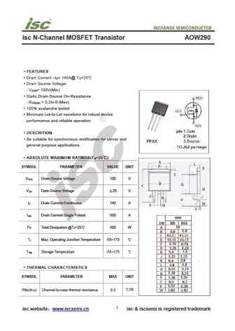
isc N-Channel MOSFET Transistor AOW290 FEATURES Drain Current I = 140A@ T =25 D C Drain Source Voltage- V = 100V(Min) DSS Static Drain-Source On-Resistance R = 3.2m (Max) DS(on) 100% avalanche tested Minimum Lot-to-Lot variations for robust device performance and reliable operation DESCRITION Be suitable for synchronous rectification for server and gene... See More ⇒
Detailed specifications: AOTF2146L
, AOTF2210L
, AOTF286L
, AOTF290L
, AOTF292L
, AOTF296L
, AOW2502
, AOW290
, IRF1405
, AOW296
, AOWF296
, AOWF190A60
, AOY2610E
, AP92T12GP
, AP95T10GP
, AP97T07GP
, AP9970GW
.
Keywords - AOW292 MOSFET specs
AOW292 cross reference
AOW292 equivalent finder
AOW292 pdf lookup
AOW292 substitution
AOW292 replacement
Need a MOSFET replacement?
Our guide shows you how to find a perfect substitute by comparing key parameters and specs