IRFW710B Specs and Replacement
Type Designator: IRFW710B
Type of Transistor: MOSFET
Type of Control Channel: N-Channel
Absolute Maximum Ratings
Pd ⓘ
- Maximum Power Dissipation: 36 W
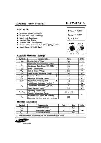
|Vds|ⓘ - Maximum Drain-Source Voltage: 400 V
|Vgs|ⓘ - Maximum Gate-Source Voltage: 30 V
|Id| ⓘ - Maximum Drain Current: 2 A
Tj ⓘ - Maximum Junction Temperature: 150 °C
Electrical Characteristics
tr ⓘ - Rise Time: 25 nS
Cossⓘ -
Output Capacitance: 30 pF
RDSonⓘ - Maximum Drain-Source On-State Resistance: 2.7 Ohm
Package: TO263
- MOSFET ⓘ Cross-Reference Search
IRFW710B datasheet
..1. Size:667K fairchild semi
irfw710b irfi710b.pdf 
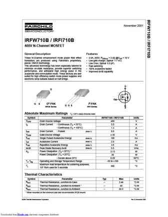
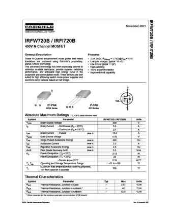
November 2001 IRFW710B / IRFI710B 400V N-Channel MOSFET General Description Features These N-Channel enhancement mode power field effect 2.0A, 400V, RDS(on) = 3.4 @VGS = 10 V transistors are produced using Fairchild s proprietary, Low gate charge ( typical 7.7 nC) planar, DMOS technology. Low Crss ( typical 6.0 pF) This advanced technology has been especially tailored t... See More ⇒
9.4. Size:679K fairchild semi
irfw740b irfi740b.pdf 
November 2001 IRFW740B / IRFI740B 400V N-Channel MOSFET General Description Features These N-Channel enhancement mode power field effect 10A, 400V, RDS(on) = 0.54 @VGS = 10 V transistors are produced using Fairchild s proprietary, Low gate charge ( typical 41 nC) planar, DMOS technology. Low Crss ( typical 35 pF) This advanced technology has been especially tailored to ... See More ⇒
9.5. Size:666K fairchild semi
irfw720b irfi720b.pdf 
November 2001 IRFW720B / IRFI720B 400V N-Channel MOSFET General Description Features These N-Channel enhancement mode power field effect 3.3A, 400V, RDS(on) = 1.75 @VGS = 10 V transistors are produced using Fairchild s proprietary, Low gate charge ( typical 14 nC) planar, DMOS technology. Low Crss ( typical 11 pF) This advanced technology has been especially tailored to... See More ⇒
9.6. Size:506K samsung
irfw720a.pdf 
Advanced Power MOSFET FEATURES BVDSS = 400 V Avalanche Rugged Technology RDS(on) = 1.8 Rugged Gate Oxide Technology Lower Input Capacitance ID = 3.3 A Improved Gate Charge Extended Safe Operating Area Lower Leakage Current 10 A (Max.) @ VDS = 400V 2 Lower RDS(ON) 1.408 (Typ.) 1 1 2 3 3 1. Gate 2. Drain 3. Source Absolute Maximum Ratings Symbol C... See More ⇒
9.7. Size:506K samsung
irfw730a.pdf 
Advanced Power MOSFET FEATURES BVDSS = 400 V Avalanche Rugged Technology RDS(on) = 1.0 Rugged Gate Oxide Technology Lower Input Capacitance ID = 5.5 A Improved Gate Charge Extended Safe Operating Area Lower Leakage Current 10 A (Max.) @ VDS = 400V 2 Lower RDS(ON) 0.765 (Typ.) 1 1 2 3 3 1. Gate 2. Drain 3. Source Absolute Maximum Ratings Symbol C... See More ⇒
9.8. Size:509K samsung
irfw740a.pdf 
Advanced Power MOSFET FEATURES BVDSS = 400 V Avalanche Rugged Technology RDS(on) = 0.55 Rugged Gate Oxide Technology Lower Input Capacitance ID = 10 A Improved Gate Charge Extended Safe Operating Area Lower Leakage Current 10 A (Max.) @ VDS = 400V 2 Lower RDS(ON) 0.437 (Typ.) 1 1 2 3 3 1. Gate 2. Drain 3. Source Absolute Maximum Ratings Symbol Cha... See More ⇒
Detailed specifications: IRLF120, IRFJ240, IRFV064, IRFV260, IRFV360, IRFV460, IRFW610B, IRFI630B, IRLZ44N, IRFI064, IRFI1010NPBF, IRFI1310NPBF, IRFI260, IRFI3205PBF, IRFI360, IRFI4110GPBF, IRFI4227PBF
Keywords - IRFW710B MOSFET specs
IRFW710B cross reference
IRFW710B equivalent finder
IRFW710B pdf lookup
IRFW710B substitution
IRFW710B replacement
Learn how to find the right MOSFET substitute. A guide to cross-reference, check specs and replace MOSFETs in your circuits.