IRFR110PBF Datasheet. Specs and Replacement
Type Designator: IRFR110PBF 📄📄
Type of Transistor: MOSFET
Type of Control Channel: N-Channel
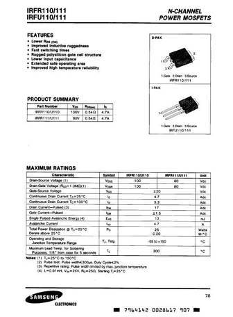
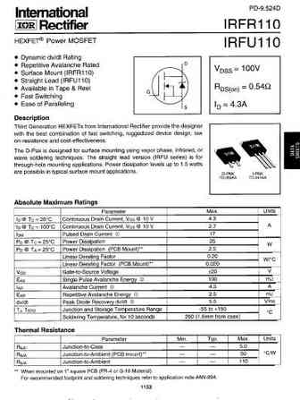
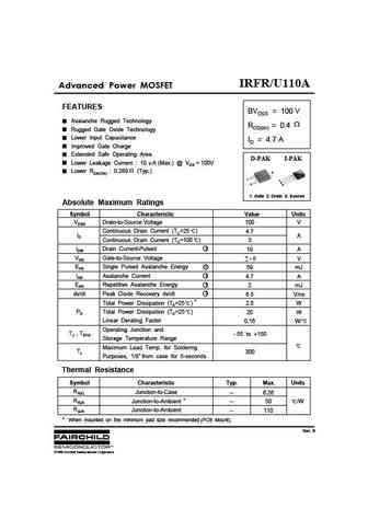
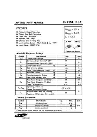
Absolute Maximum Ratings
Pd ⓘ - Maximum Power Dissipation: 25 W
|Vds|ⓘ - Maximum Drain-Source Voltage: 100 V
|Vgs|ⓘ - Maximum Gate-Source Voltage: 20 V
|Id| ⓘ - Maximum Drain Current: 4.3 A
Tj ⓘ - Maximum Junction Temperature: 150 °C
Electrical Characteristics
tr ⓘ - Rise Time: 16 nS
Cossⓘ - Output Capacitance: 80 pF
RDSonⓘ - Maximum Drain-Source On-State Resistance: 0.54 Ohm
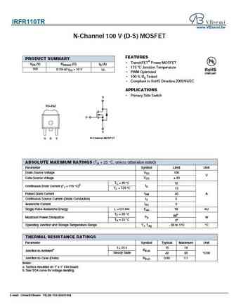
Package: TO252
📄📄 Copy
IRFR110PBF substitution
- MOSFET ⓘ Cross-Reference Search
IRFR110PBF datasheet
irfr110pbf irfu110pbf.pdf
PD - 95026A IRFR110PbF IRFU110PbF Lead-Free 12/14/04 Document Number 91265 www.vishay.com 1 IRFR/U110PbF Document Number 91265 www.vishay.com 2 IRFR/U110PbF Document Number 91265 www.vishay.com 3 IRFR/U110PbF Document Number 91265 www.vishay.com 4 IRFR/U110PbF Document Number 91265 www.vishay.com 5 IRFR/U110PbF Document Number 91265 www.vishay.com 6 IRFR/U1... See More ⇒
irfr110pbf sihfr110.pdf

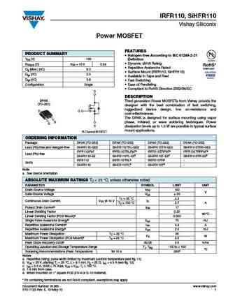
IRFR110, SiHFR110 Vishay Siliconix Power MOSFET FEATURES PRODUCT SUMMARY Halogen-free According to IEC 61249-2-21 VDS (V) 100 Definition Dynamic dV/dt Rating RDS(on) ( )VGS = 10 V 0.54 Repetitive Avalanche Rated Qg (Max.) (nC) 8.3 Surface Mount (IRFR110, SiHFR110) Qgs (nC) 2.3 Available in Tape and Reel Qgd (nC) 3.8 Fast Switching Configuration Single ... See More ⇒
Detailed specifications: IRFB812PBF, IRFR010PBF, IRFR014PBF, IRFR020PBF, IRFR024NPBF, IRFR024PBF, IRFR1010ZPBF, IRFR1018EPBF, AO4468, IRFR1205PBF, IRFR120ATM, IRFR120NPBF, IRFR120PBF, IRFR120ZPBF, IRFR12N25DPBF, IRFR130ATM, IRFR13N15DPBF
Keywords - IRFR110PBF MOSFET specs
IRFR110PBF cross reference
IRFR110PBF equivalent finder
IRFR110PBF pdf lookup
IRFR110PBF substitution
IRFR110PBF replacement
Learn how to find the right MOSFET substitute. A guide to cross-reference, check specs and replace MOSFETs in your circuits.
MOSFET Parameters. How They Affect Each Other
🌐 : EN ES РУ

LIST
Last Update
MOSFET: CEZC2P07 | CEZ2R05 | CEU3133 | CES2361 | CES2312A | CEP100N10L | CEM3425 | CEM3139 | CEM3133 | CEM3115
Popular searches
irf740 datasheet | ksa992 | irfb4227 | irfb4110 | tip36c | bd139 transistor | irf840 datasheet | ge10001