SI2304DDS Specs and Replacement
Type Designator: SI2304DDS
Type of Transistor: MOSFET
Type of Control Channel: N-Channel
Absolute Maximum Ratings
Pd ⓘ - Maximum Power Dissipation: 1.1 W
|Vds|ⓘ - Maximum Drain-Source Voltage: 30 V
|Vgs|ⓘ - Maximum Gate-Source Voltage: 20 V
|Id| ⓘ - Maximum Drain Current: 3.3 A
Tj ⓘ - Maximum Junction Temperature: 150 °C
Electrical Characteristics
tr ⓘ - Rise Time: 50 nS
Cossⓘ - Output Capacitance: 45 pF
RDSonⓘ - Maximum Drain-Source On-State Resistance: 0.06 Ohm
Package: SOT-23
SI2304DDS substitution
- MOSFET ⓘ Cross-Reference Search
SI2304DDS datasheet
si2304dds.pdf
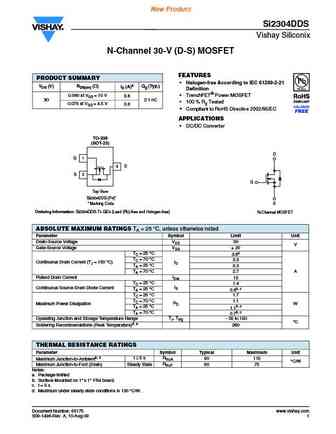
New Product Si2304DDS Vishay Siliconix N-Channel 30-V (D-S) MOSFET FEATURES PRODUCT SUMMARY Halogen-free According to IEC 61249-2-21 VDS (V) RDS(on) ( ) ID (A)a Qg (Typ.) Definition 0.060 at VGS = 10 V TrenchFET Power MOSFET 3.6 30 2.1 nC 100 % Rg Tested 0.075 at VGS = 4.5 V 3.6 Compliant to RoHS Directive 2002/95/EC APPLICATIONS DC/DC Converter T... See More ⇒
si2304dd.pdf

New Product Si2304DDS Vishay Siliconix N-Channel 30-V (D-S) MOSFET FEATURES PRODUCT SUMMARY Halogen-free According to IEC 61249-2-21 VDS (V) RDS(on) ( ) ID (A)a Qg (Typ.) Definition 0.060 at VGS = 10 V TrenchFET Power MOSFET 3.6 30 2.1 nC 100 % Rg Tested 0.075 at VGS = 4.5 V 3.6 Compliant to RoHS Directive 2002/95/EC APPLICATIONS DC/DC Converter T... See More ⇒
si2304ds.pdf
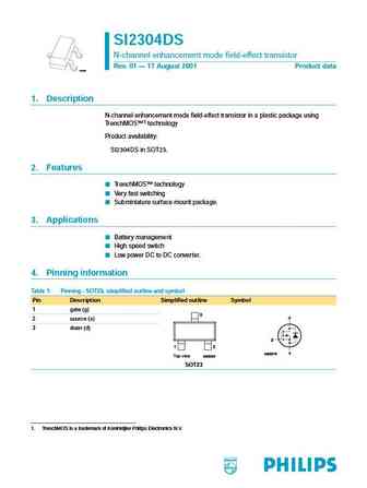
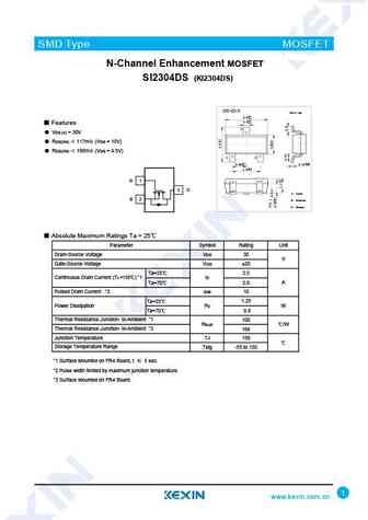
SI2304DS N-channel enhancement mode field-effect transistor Rev. 01 17 August 2001 Product data M3D088 1. Description N-channel enhancement mode field-effect transistor in a plastic package using TrenchMOS 1 technology Product availability SI2304DS in SOT23. 2. Features TrenchMOS technology Very fast switching Subminiature surface mount package. 3. Applications Batte... See More ⇒
si2304ds.pdf
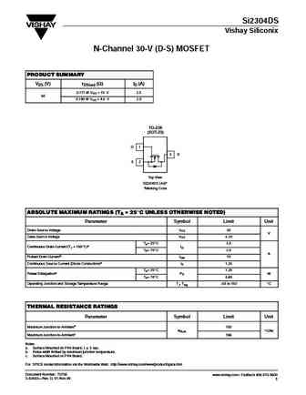
Si2304DS Vishay Siliconix N-Channel 30-V (D-S) MOSFET PRODUCT SUMMARY VDS (V) rDS(on) (W) ID (A) 0.117 @ VGS = 10 V 2.5 30 30 0.190 @ VGS = 4.5 V 2.0 TO-236 (SOT-23) G 1 3 D S 2 Top View Si2304DS (A4)* *Marking Code ABSOLUTE MAXIMUM RATINGS (TA = 25_C UNLESS OTHERWISE NOTED) Parameter Symbol Limit Unit Drain-Source Voltage VDS 30 V V Gate-Source Voltage VGS "20 TA= 25_C 2... See More ⇒
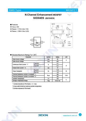

Detailed specifications: SI2301-TP, SI2302ADS, SI2302ADS-T1, SI2302CDS, SI2302DDS, SI2302-TP, SI2303CDS, SI2304BDS, 2SK3568, SI2305ADS, SI2305CDS, SI2306BDS, SI2307CDS, SI2308BDS, SI2309CDS, SI2311DS, SI2312BDS
Keywords - SI2304DDS MOSFET specs
SI2304DDS cross reference
SI2304DDS equivalent finder
SI2304DDS pdf lookup
SI2304DDS substitution
SI2304DDS replacement
Can't find your MOSFET? Learn how to find a substitute transistor by analyzing voltage, current and package compatibility
History: AOD442 | FQD1N80 | JMSL1040AU | VSP007N07MS
🌐 : EN ES РУ

LIST
Last Update
MOSFET: AUB062N08BG | AUB060N08AG | AUB056N10 | AUB056N08BGL | AUB050N085 | AUB050N055 | AUB045N12 | AUB045N10BT | AUB039N10 | AUB034N10
Popular searches
bc639 equivalent | bd138 transistor equivalent | c1096 transistor | c1345 transistor | jcs640c | kn2907a | ncep028n85 datasheet | sw50n06