SSF2641S Datasheet. Specs and Replacement
Type Designator: SSF2641S 📄📄
Type of Transistor: MOSFET
Type of Control Channel: P-Channel
Absolute Maximum Ratings
Pd ⓘ - Maximum Power Dissipation: 5 W
|Vds|ⓘ - Maximum Drain-Source Voltage: 20 V
|Vgs|ⓘ - Maximum Gate-Source Voltage: 12 V
|Id| ⓘ - Maximum Drain Current: 7.9 A
Tj ⓘ - Maximum Junction Temperature: 150 °C
Electrical Characteristics
tr ⓘ - Rise Time: 7 nS
Cossⓘ - Output Capacitance: 150 pF
RDSonⓘ - Maximum Drain-Source On-State Resistance: 0.05 Ohm
Package: SOP-8
SSF2641S substitution
- MOSFET ⓘ Cross-Reference Search
SSF2641S datasheet
ssf2641s.pdf
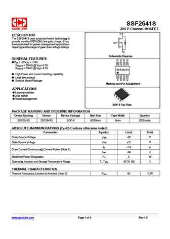
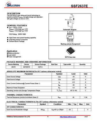
SSF2641S 20V P-Channel MOSFET D DESCRIPTION The SSF2641S uses advanced trench technology to provide excellent RDS(ON), low gate charge. It has G been optimized for power management applications requiring a wide range of gave drive voltage ratings. S Schematic Diagram GENERAL FEATURES VDS = -20V,ID = -7.9A RDS(ON) ... See More ⇒
ssf2649.pdf
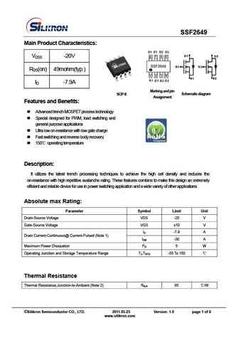
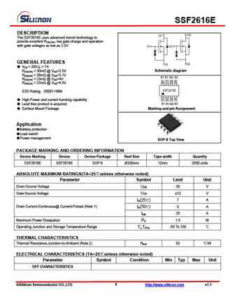
SSF2649 Main Product Characteristics D1 D2 VDSS -20V G1 G2 RDS(on) 49mohm(typ.) S1 S2 ID -7.9A Marking and pin SOP-8 Schematic diagram Assignment Features and Benefits Advanced trench MOSFET process technology Special designed for PWM, load switching and general purpose applications Ultra low on-resistance with low gate charge Fast switching and re... See More ⇒
ssf2627.pdf
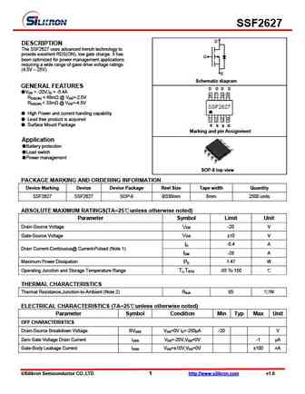
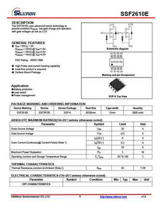
SSF2627 D DESCRIPTION The SSF2627 uses advanced trench technology to provide excellent RDS(ON), low gate charge. It has G been optimized for power management applications requiring a wide range of gave drive voltage ratings (4.5V 25V). S Schematic diagram GENERAL FEATURES VDS = -20V,ID = -5.4A RDS(ON) ... See More ⇒
ssf26ns60a.pdf
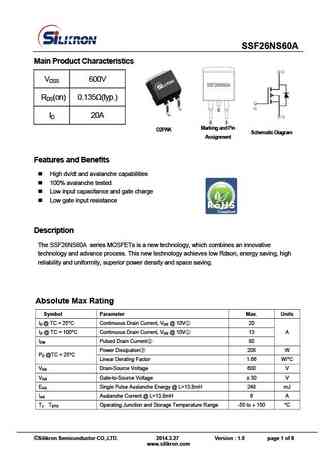
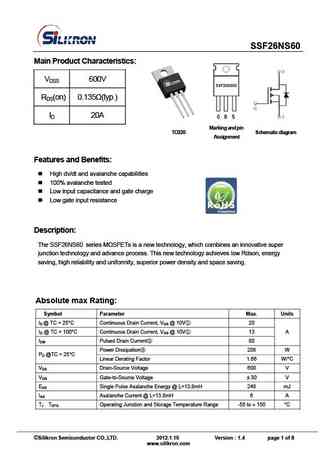
SSF26NS60A Main Product Characteristics VDSS 600V RDS(on) 0.135 (typ.) ID 20A Marking and Pin D2PAK Schematic Diagram Assignment Features and Benefits High dv/dt and avalanche capabilities 100% avalanche tested Low input capacitance and gate charge Low gate input resistance Description The SSF26NS60A series MOSFETs is a new technology, which combines... See More ⇒
Detailed specifications: SQR40N10-25, SQR50N03-06P, SQR50N04-3M8, SQR50N06-07L, SSF22A5E, SSF2418B, SSF2418EBK, SSF2439E, 2N60, SSF2816EBK, SSF2N60D1, SSF3612E, R9523, SSF440M, SSF450M, SSF5508D, SSF5510G
Keywords - SSF2641S MOSFET specs
SSF2641S cross reference
SSF2641S equivalent finder
SSF2641S pdf lookup
SSF2641S substitution
SSF2641S replacement
Can't find your MOSFET? Learn how to find a substitute transistor by analyzing voltage, current and package compatibility
🌐 : EN ES РУ

LIST
Last Update
MOSFET: ASDM30P100KQ | ASDM30N90Q | ASDM30N75KQ | ASDM30N150Q | ASDM30N120Q | ASDM30N120KQ | ASDM30N100KQ | ASDM30DN40E | ASDM30DN30E | ASDM3050KQ
Popular searches
d2390 datasheet | 2sa750 replacement | 2sc984 replacement | a1046 transistor | hy19p03 | 2sk2749 | c2577 transistor | k3563 transistor