TMPF16N25Z Datasheet. Specs and Replacement
Type Designator: TMPF16N25Z 📄📄
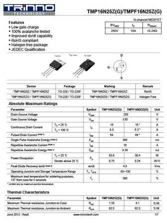
Type of Transistor: MOSFET
Type of Control Channel: N-Channel
Absolute Maximum Ratings
Pd ⓘ - Maximum Power Dissipation: 30.4 W
|Vds|ⓘ - Maximum Drain-Source Voltage: 250 V
|Vgs|ⓘ - Maximum Gate-Source Voltage: 30 V
|Id| ⓘ - Maximum Drain Current: 16 A
Tj ⓘ - Maximum Junction Temperature: 150 °C
Electrical Characteristics
tr ⓘ - Rise Time: 51 nS
Cossⓘ - Output Capacitance: 152 pF
RDSonⓘ - Maximum Drain-Source On-State Resistance: 0.24 Ohm
Package: TO-220F
📄📄 Copy
- MOSFET ⓘ Cross-Reference Search
TMPF16N25Z datasheet
7.1. Size:618K trinnotech
tmp16n60a tmpf16n60a.pdf 
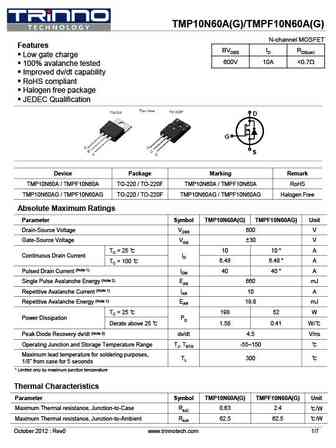
TMP16N60A(G)/TMPF16N60A(G) Features N-channel MOSFET Low gate charge BVDSS ID RDS(on) 100% avalanche tested 600V 16A ... See More ⇒
7.2. Size:341K trinnotech
tmp16n60 tmpf16n60.pdf

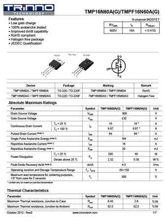
TMP16N60/TMPF16N60 TMP16N60G/TMPF16N60G VDSS = 660 V @Tjmax Features ID = 16A Low gate charge RDS(on) = 0.47 W(max) @ VGS= 10 V 100% avalanche tested Improved dv/dt capability RoHS compliant Halogen free package JEDEC Qualification D G S Device Package Marking Remark TMP16N60 / TMPF16N60 TO-220 / TO-220F TMP16N60 / TMPF16N60 RoHS TMP16N60G / TMPF16N60G... See More ⇒
9.1. Size:609K trinnotech
tmp10n80 tmpf10n80.pdf
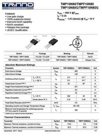
TMP10N80/TMPF10N80 TMP10N80G/TMPF10N80G VDSS = 880 V @Tjmax Features ID = 9.5A Low gate charge RDS(ON) = 1.05 W(max) @ VGS= 10 V 100% avalanche tested Improved dv/dt capability RoHS compliant Halogen free package JEDEC Qualification D G S Device Package Marking Remark TMP10N80 / TMPF10N80 TO-220 / TO-220F TMP10N80 / TMPF10N80 RoHS TMP10N... See More ⇒
9.3. Size:336K trinnotech
tmp13n50 tmpf13n50.pdf

TMP13N50/TMPF13N50 TMP13N50G/TMPF13N50G VDSS = 550 V @Tjmax Features ID = 13A Low gate charge RDS(on) = 0.48 W(max) @ VGS= 10 V 100% avalanche tested Improved dv/dt capability RoHS compliant Halogen free package JEDEC Qualification D G S Device Package Marking Remark TMP13N50 / TMPF13N50 TO-220 / TO-220F TMP13N50 / TMPF13N50 RoHS TMP13N50G / TMPF13N50G... See More ⇒
9.4. Size:340K trinnotech
tmp11n50sg tmpf11n50sg.pdf
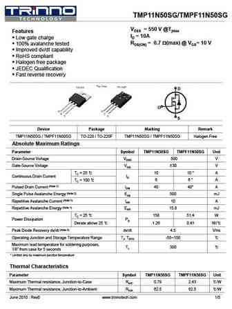
TMP11N50SG/TMPF11N50SG VDSS = 550 V @Tjmax Features ID = 10A Low gate charge RDS(ON) = 0.7 W(max) @ VGS= 10 V 100% avalanche tested Improved dv/dt capability RoHS compliant Halogen free package JEDEC Qualification Fast reverse recovery D G S Device Package Marking Remark TMP11N50SG / TMPF11N50SG TO-220 / TO-220F TMP11N50SG / TMPF11N50SG Halogen Fre... See More ⇒
9.5. Size:591K trinnotech
tmp18n20z tmpf18n20z.pdf
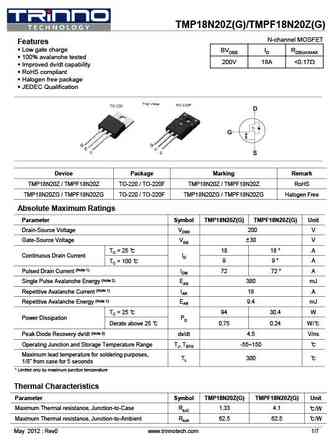
TMP18N20Z(G)/TMPF18N20Z(G) N-channel MOSFET Features Low gate charge BVDSS ID RDS(on)MAX 100% avalanche tested 200V 18A ... See More ⇒
9.7. Size:335K trinnotech
tmp10n60 tmpf10n60.pdf
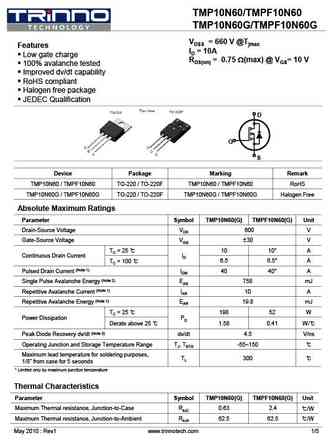
TMP10N60/TMPF10N60 TMP10N60G/TMPF10N60G VDSS = 660 V @Tjmax Features ID = 10A Low gate charge RDS(on) = 0.75 W(max) @ VGS= 10 V 100% avalanche tested Improved dv/dt capability RoHS compliant Halogen free package JEDEC Qualification D G S Device Package Marking Remark TMP10N60 / TMPF10N60 TO-220 / TO-220F TMP10N60 / TMPF10N60 RoHS TMP10N60G / TMPF10N60G... See More ⇒
9.8. Size:577K trinnotech
tmp10n65 tmpf10n65.pdf
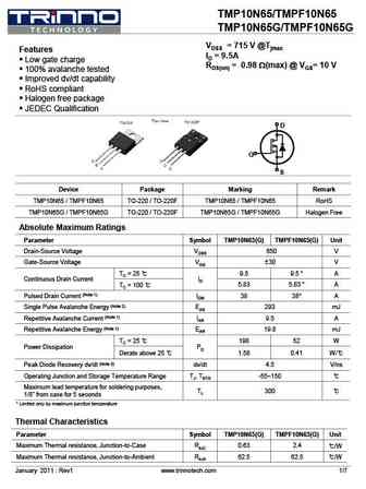
TMP10N65/TMPF10N65 TMP10N65G/TMPF10N65G VDSS = 715 V @Tjmax Features ID = 9.5A Low gate charge RDS(on) = 0.98 W(max) @ VGS= 10 V 100% avalanche tested Improved dv/dt capability RoHS compliant Halogen free package JEDEC Qualification D G S Device Package Marking Remark TMP10N65 / TMPF10N65 TO-220 / TO-220F TMP10N65 / TMPF10N65 RoHS TMP10N... See More ⇒
9.9. Size:332K trinnotech
tmp12n60 tmpf12n60.pdf

TMP12N60/TMPF12N60 TMP12N60G/TMPF12N60G VDSS = 660 V @Tjmax Features ID = 12A Low gate charge RDS(on) = 0.65 W(max) @ VGS= 10 V 100% avalanche tested Improved dv/dt capability RoHS compliant Halogen free package JEDEC Qualification D G S Device Package Marking Remark TMP12N60 / TMPF12N60 TO-220 / TO-220F TMP12N60 / TMPF12N60 RoHS TMP12N60G / TMPF12N60G... See More ⇒
9.10. Size:353K trinnotech
tmp11n50 tmpf11n50.pdf
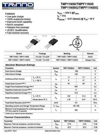
TMP11N50/TMPF11N50 TMP11N50G/TMPF11N50G VDSS = 550 V @Tjmax Features ID = 11A Low gate charge RDS(ON) = 0.67 W(max) @ VGS= 10 V 100% avalanche tested Improved dv/dt capability RoHS compliant Halogen free package JEDEC Qualification Fast reverse recovery D G S Device Package Marking Remark TMP11N50 / TMPF11N50 TO-220 / TO-220F TMP11N50 / TMPF11N50 ... See More ⇒
9.11. Size:343K trinnotech
tmp15n50 tmpf15n50.pdf

TMP15N50/TMPF15N50 TMP15N50G/TMPF15N50G VDSS = 550 V @Tjmax Features ID = 14A Low gate charge RDS(on) = 0.44 W(max) @ VGS= 10 V 100% avalanche tested Improved dv/dt capability RoHS compliant Halogen free package JEDEC Qualification D G S Device Package Marking Remark TMP15N50 / TMPF15N50 TO-220 / TO-220F TMP15N50 / TMPF15N50 RoHS TMP15N50G / TMPF15N50G... See More ⇒
9.13. Size:429K trinnotech
tmpf13n50a.pdf
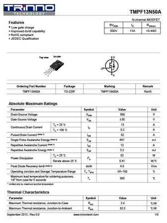
TMPF13N50A N-channel MOSFET Features BVDSS ID RDS(on) Low gate charge 500V 13A ... See More ⇒
Detailed specifications: TMPF10N80, TMPF11N50, TMPF11N50SG, TMPF12N60, TMPF12N60A, TMPF13N50, TMPF13N50A, TMPF15N50, IRF3205, TMPF16N60, TMPF16N60A, TMPF18N20Z, TMPF20N50, TMPF20N50A, TMPF2N60AZ, TMPF2N60Z, TMPF2N65AZ
Keywords - TMPF16N25Z MOSFET specs
TMPF16N25Z cross reference
TMPF16N25Z equivalent finder
TMPF16N25Z pdf lookup
TMPF16N25Z substitution
TMPF16N25Z replacement
Learn how to find the right MOSFET substitute. A guide to cross-reference, check specs and replace MOSFETs in your circuits.