TMU3N40ZG Datasheet. Specs and Replacement
Type Designator: TMU3N40ZG 📄📄
Type of Transistor: MOSFET
Type of Control Channel: N-Channel
Absolute Maximum Ratings
Pd ⓘ - Maximum Power Dissipation: 30 W
|Vds|ⓘ - Maximum Drain-Source Voltage: 400 V
|Vgs|ⓘ - Maximum Gate-Source Voltage: 30 V
|Id| ⓘ - Maximum Drain Current: 2 A
Tj ⓘ - Maximum Junction Temperature: 150 °C
Electrical Characteristics
tr ⓘ - Rise Time: 9 nS
Cossⓘ - Output Capacitance: 32 pF
RDSonⓘ - Maximum Drain-Source On-State Resistance: 3.4 Ohm
Package: I-PAK
📄📄 Copy
TMU3N40ZG substitution
- MOSFET ⓘ Cross-Reference Search
TMU3N40ZG datasheet
tmd3n40zg tmu3n40zg.pdf
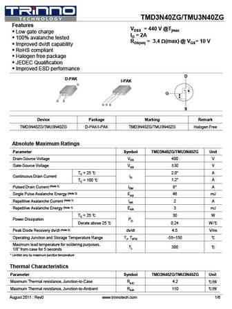
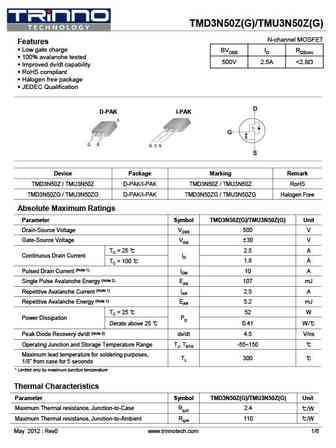
TMD3N40ZG/TMU3N40ZG Features VDSS = 440 V @Tjmax Low gate charge ID = 2A 100% avalanche tested RDS(on) = 3.4 W(max) @ VGS= 10 V Improved dv/dt capability RoHS compliant Halogen free package JEDEC Qualification Improved ESD performance D D-PAK I-PAK G S Device Package Marking Remark TMD3N40ZG/TMU3N40ZG D-PAK/I-PAK TMD3N40ZG/TMU3N40ZG Halogen Free ... See More ⇒
tmd3n80g tmu3n80g.pdf
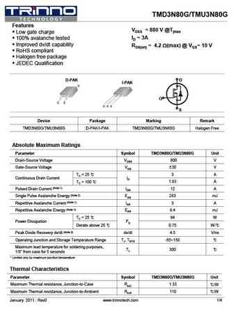
TMD3N80G/TMU3N80G Features VDSS = 880 V @Tjmax Low gate charge ID = 3A 100% avalanche tested Improved dv/dt capability RDS(on) = 4.2 W(max) @ VGS= 10 V RoHS compliant Halogen free package JEDEC Qualification D-PAK D I-PAK G S Device Package Marking Remark TMD3N80G/TMU3N80G D-PAK/I-PAK TMD3N80G/TMU3N80G Halogen Free Absolute Maximum Ratings Parameter ... See More ⇒
tmd3n90 tmu3n90.pdf
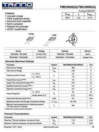
TMD3N90(G)/TMU3N90(G) N-channel MOSFET Features BVDSS ID RDS(on) Low gate charge 900V 2.5A ... See More ⇒
tmd3n50az tmu3n50az.pdf
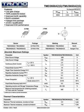
TMD3N50AZ(G)/TMU3N50AZ(G) N-channel MOSFET Features Low gate charge BVDSS ID RDS(on) 100% avalanche tested 500V 2.5A ... See More ⇒
Detailed specifications: TMT3N30G, TMT3N40ZG, TMU16N25Z, TMU18N20Z, TMU2N40, TMU2N60AZ, TMU2N60Z, TMU2N65AZ, AON7506, TMU3N50AZ, TMU3N50Z, TMU3N80G, TMU3N90, TMU4N60, TMU4N60AZ, TMU4N65AZ, TMU4N65Z
Keywords - TMU3N40ZG MOSFET specs
TMU3N40ZG cross reference
TMU3N40ZG equivalent finder
TMU3N40ZG pdf lookup
TMU3N40ZG substitution
TMU3N40ZG replacement
Need a MOSFET replacement? Our guide shows you how to find a perfect substitute by comparing key parameters and specs
