2SJ211 Specs and Replacement
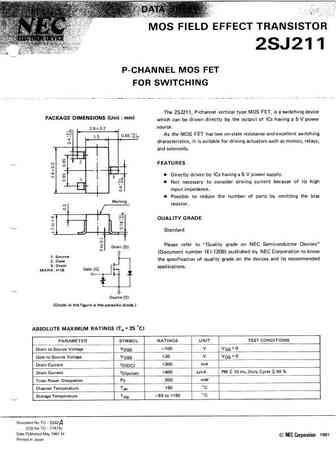
Type Designator: 2SJ211
Type of Transistor: MOSFET
Type of Control Channel: P-Channel
Absolute Maximum Ratings
Pd ⓘ
- Maximum Power Dissipation: 0.2 W
|Vds|ⓘ - Maximum Drain-Source Voltage: 100 V
|Vgs|ⓘ - Maximum Gate-Source Voltage: 20 V
|Id| ⓘ - Maximum Drain Current: 0.2 A
Tj ⓘ - Maximum Junction Temperature: 150 °C
Electrical Characteristics
tr ⓘ - Rise Time: 150 nS
Cossⓘ -
Output Capacitance: 16 pF
Rds ⓘ - Maximum Drain-Source On-State Resistance: 20 Ohm
Package: SC59
- MOSFET ⓘ Cross-Reference Search
2SJ211 datasheet
..2. Size:1220K kexin
2sj211.pdf 

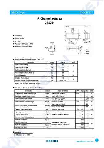
SMD Type MOSFET P-Channel MOSFET 2SJ211 SOT-23 Unit mm +0.1 2.9 -0.1 +0.1 0.4-0.1 3 Features VDS (V) =-100V 1 2 ID =-0.2 A +0.1 +0.05 0.95 -0.1 0.1 -0.01 +0.1 1.9 -0.1 RDS(ON) 20 (VGS =-10V) RDS(ON) 30 (VGS =-4V) 1. Gate 2. Source 3. Drain Absolute Maximum Ratings Ta = 25 Parameter Symbol Rating Unit Drain-Source Voltage VDS... See More ⇒
0.1. Size:1228K kexin
2sj211-3.pdf 

SMD Type MOSFET P-Channel MOSFET 2SJ211 SOT-23-3 Unit mm +0.2 2.9 -0.1 +0.1 0.4 -0.1 3 Features VDS (V) =-100V 1 2 +0.02 ID =-0.2 A +0.1 0.15 -0.02 0.95 -0.1 +0.1 1.9 -0.2 RDS(ON) 20 (VGS =-10V) RDS(ON) 30 (VGS =-4V) 1. Gate 2. Source 3. Drain Absolute Maximum Ratings Ta = 25 Parameter Symbol Rating Unit Drain-Source Voltage... See More ⇒
9.1. Size:32K 1
2sj218.pdf 

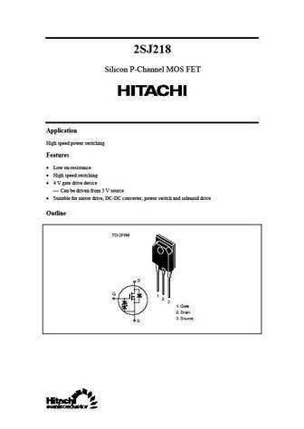
2SJ218 Silicon P-Channel MOS FET Application High speed power switching Features Low on-resistance High speed switching 4 V gate drive device Can be driven from 5 V source Suitable for motor drive, DC-DC converter, power switch and solenoid drive Outline 2SJ218 Absolute Maximum Ratings (Ta = 25 C) Item Symbol Ratings Unit Drain to source voltage VDSS 60 V ... See More ⇒
9.2. Size:29K 1
2sj216.pdf 

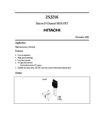
2SJ216 Silicon P-Channel MOS FET November 1996 Application High speed power switching Features Low on-resistance High speed switching Low drive current 4 V gate drive device _ Can be driven from 5 V source Suitable for motor drive, DC-DC converter, power switch and solenoid drive Outline TO-3PFM D G 1 2 3 1. Gate 2. Drain 3. Source S 2SJ216 Absolut... See More ⇒
9.3. Size:82K renesas
2sj217.pdf 

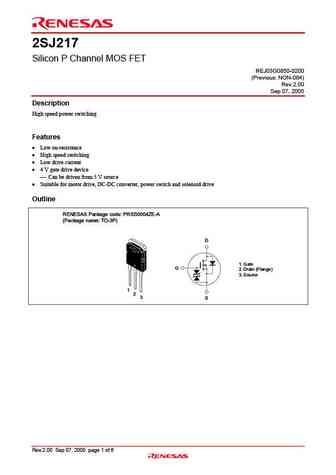
2SJ217 Silicon P Channel MOS FET REJ03G0850-0200 (Previous NON-084) Rev.2.00 Sep 07, 2005 Description High speed power switching Features Low on-resistance High speed switching Low drive current 4 V gate drive device Can be driven from 5 V source Suitable for motor drive, DC-DC converter, power switch and solenoid drive Outline RENESAS Pa... See More ⇒
9.4. Size:95K renesas
rej03g0850 2sj217ds.pdf 

To our customers, Old Company Name in Catalogs and Other Documents On April 1st, 2010, NEC Electronics Corporation merged with Renesas Technology Corporation, and Renesas Electronics Corporation took over all the business of both companies. Therefore, although the old company name remains in this document, it is a valid Renesas Electronics document. We appreciate your understanding. ... See More ⇒
9.5. Size:152K renesas
2sj210c.pdf 

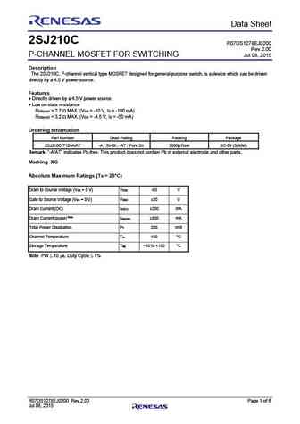
Preliminary Data Sheet 2SJ210C R07DS1278EJ0200 Rev.2.00 P-CHANNEL MOSFET FOR SWITCHING Jul 08, 2015 Description The 2SJ210C, P-channel vertical type MOSFET designed for general-purpose switch, is a device which can be driven directly by a 4.5 V power source. Features Directly driven by a 4.5 V power source. Low on-state resistance RDS(on)1 = 2.7 MAX. (VGS = -10 ... See More ⇒
9.9. Size:58K hitachi
2sj215.pdf 

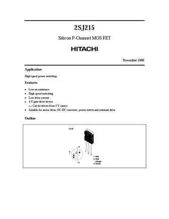
2SJ215 Silicon P-Channel MOS FET November 1996 Application High speed power switching Features Low on-resistance High speed switching Low drive current 4 V gate drive device Can be driven from 5 V source Suitable for motor drive, DC-DC converter, power switch and solenoid drive Outline TO-3P D 1 G 2 3 1. Gate 2. Drain (Flange) S 3. Source 2SJ2... See More ⇒
9.11. Size:1034K kexin
2sj213.pdf 

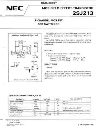
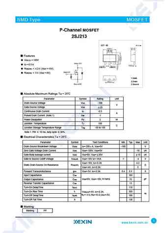
SMD Type MOSFET P-Channel MOSFET 2SJ213 1.70 0.1 Features VDS (V) =-100V ID =-0.5 A 0.42 0.1 0.46 0.1 RDS(ON) 4.2 (VGS =-10V) RDS(ON) 5 (VGS =-4V) 1.Gate 2.Drain 3.Source Absolute Maximum Ratings Ta = 25 Parameter Symbol Rating Unit Drain-Source Voltage VDS -100 V Gate-Source Voltage VGS 20 Continuous Drain Current ID -0.5 A ... See More ⇒
9.12. Size:964K kexin
2sj210.pdf 

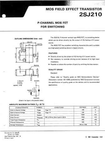
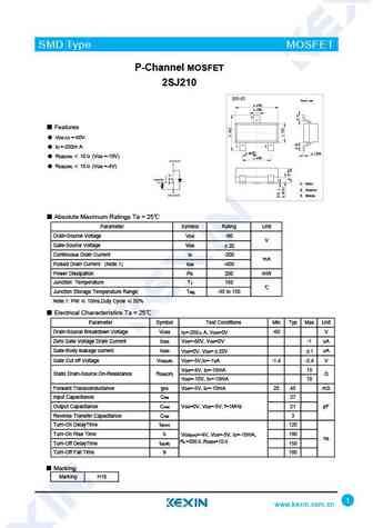
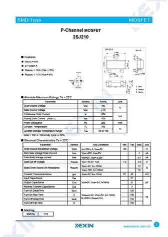
SMD Type MOSFET P-Channel MOSFET 2SJ210 SOT-23 Unit mm +0.1 2.9 -0.1 +0.1 0.4 -0.1 3 Features VDS (V) =-60V 1 2 ID =-200m A +0.1 +0.05 0.95-0.1 0.1-0.01 RDS(ON) 10 (VGS =-10V) +0.1 1.9-0.1 RDS(ON) 15 (VGS =-4V) 1. Gate 2. Source 3. Drain Absolute Maximum Ratings Ta = 25 Parameter Symbol Rating Unit Drain-Source Voltage VDS -6... See More ⇒
9.13. Size:1256K kexin
2sj210-3.pdf 

SMD Type MOSFET P-Channel MOSFET 2SJ210 SOT-23-3 Unit mm +0.2 2.9 -0.1 +0.1 0.4 -0.1 Features 3 VDS (V) =-60V ID =-200m A RDS(ON) 10 (VGS =-10V) 1 2 +0.02 +0.1 0.15 -0.02 0.95-0.1 RDS(ON) 15 (VGS =-4V) +0.1 1.9-0.2 1. Gate 2. Source 3. Drain Absolute Maximum Ratings Ta = 25 Parameter Symbol Rating Unit Drain-Source Voltage VD... See More ⇒
9.14. Size:1308K kexin
2sj212.pdf 

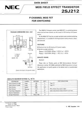
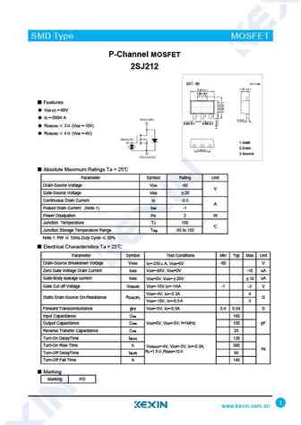
SMD Type MOSFET P-Channel MOSFET 2SJ212 1.70 0.1 Features VDS (V) =-60V ID =-500m A 0.42 0.1 0.46 0.1 RDS(ON) 3 (VGS =-10V) RDS(ON) 4 (VGS =-4V) 1.Gate 2.Drain 3.Source Absolute Maximum Ratings Ta = 25 Parameter Symbol Rating Unit Drain-Source Voltage VDS -60 V Gate-Source Voltage VGS 20 Continuous Drain Current ID -0.5 A Pul... See More ⇒
Detailed specifications: 2SJ203
, 2SJ204
, 2SJ205
, 2SJ206
, 2SJ207
, 2SJ208
, 2SJ209
, 2SJ210
, K4145
, 2SJ212
, 2SJ218
, 2SJ243
, 2SJ302
, 2SJ303
, 2SJ324
, 2SJ325
, 2SJ326
.
Keywords - 2SJ211 MOSFET specs
2SJ211 cross reference
2SJ211 equivalent finder
2SJ211 pdf lookup
2SJ211 substitution
2SJ211 replacement
Can't find your MOSFET?
Learn how to find a substitute transistor by analyzing voltage, current and package compatibility


