FMI16N50ES Specs and Replacement
Type Designator: FMI16N50ES
Type of Transistor: MOSFET
Type of Control Channel: N-Channel
Absolute Maximum Ratings
Pd ⓘ - Maximum Power Dissipation: 225 W
|Vds|ⓘ - Maximum Drain-Source Voltage: 500 V
|Vgs|ⓘ - Maximum Gate-Source Voltage: 30 V
|Id| ⓘ - Maximum Drain Current: 16 A
Tj ⓘ - Maximum Junction Temperature: 150 °C
Electrical Characteristics
tr ⓘ - Rise Time: 30 nS
Cossⓘ - Output Capacitance: 210 pF
RDSonⓘ - Maximum Drain-Source On-State Resistance: 0.38 Ohm
Package: T-PACK-L
FMI16N50ES substitution
- MOSFET ⓘ Cross-Reference Search
FMI16N50ES datasheet
fmi16n50es.pdf
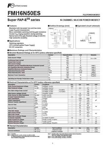
FMI16N50ES FUJI POWER MOSFET Super FAP-E3S series N-CHANNEL SILICON POWER MOSFET Features Outline Drawings [mm] Equivalent circuit schematic Maintains both low power loss and low noise T-Pack (L) Lower R (on) characteristic DS More controllable switching dv/dt by gate resistance Drain(D) Smaller V ringing waveform during switching GS Narrow band of the gate threshold voltage (4.2 0.... See More ⇒
fmi16n50e.pdf
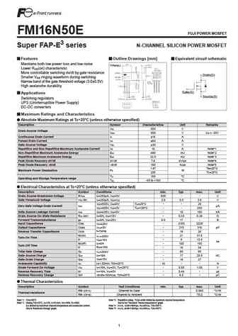
FMI16N50E FUJI POWER MOSFET Super FAP-E3 series N-CHANNEL SILICON POWER MOSFET Features Outline Drawings [mm] Equivalent circuit schematic Maintains both low power loss and low noise T-Pack(L) Lower R (on) characteristic DS More controllable switching dv/dt by gate resistance Drain(D) Smaller V ringing waveform during switching GS Narrow band of the gate threshold voltage (3.0 0.5V)... See More ⇒
fmi16n60es.pdf
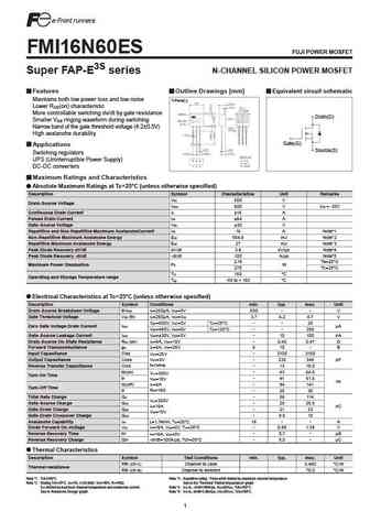
FMI16N60ES FUJI POWER MOSFET Super FAP-E3S series N-CHANNEL SILICON POWER MOSFET Features Outline Drawings [mm] Equivalent circuit schematic Maintains both low power loss and low noise T-Pack(L) Lower R (on) characteristic DS More controllable switching dv/dt by gate resistance Drain(D) Smaller V ringing waveform during switching GS Narrow band of the gate threshold voltage (4.2 0.5... See More ⇒
fmi16n60e.pdf
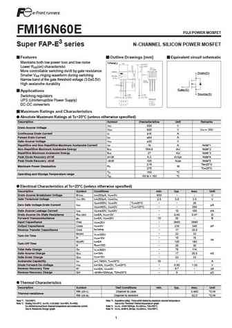
FMI16N60E FUJI POWER MOSFET Super FAP-E3 series N-CHANNEL SILICON POWER MOSFET Features Outline Drawings [mm] Equivalent circuit schematic Maintains both low power loss and low noise T-Pack(L) Lower R (on) characteristic DS More controllable switching dv/dt by gate resistance Drain(D) Smaller V ringing waveform during switching GS Narrow band of the gate threshold voltage (3.0 0.5V)... See More ⇒
Detailed specifications: FMI10N60E, FMI11N60E, FMI12N50E, FMI12N50ES, FMI12N60ES, FMI13N60E, FMI13N60ES, FMI16N50E, IRFP250N, FMI16N60E, FMI16N60ES, FMI20N50E, FMI20N50ES, FMI80N10T2, FML12N50ES, FML12N60ES, FML13N60ES
Keywords - FMI16N50ES MOSFET specs
FMI16N50ES cross reference
FMI16N50ES equivalent finder
FMI16N50ES pdf lookup
FMI16N50ES substitution
FMI16N50ES replacement
Can't find your MOSFET? Learn how to find a substitute transistor by analyzing voltage, current and package compatibility
🌐 : EN ES РУ

LIST
Last Update
MOSFET: CM4407 | CM3407 | CM3400 | SVF11N65F | SVF11N65T | FKBB3105 | EHBA036R1 | CRTT067N10N | AP6NA3R2MT | AP65SA145DDT8
Popular searches
b649a transistor | 2sa606 | 2n3644 | 2sc2240bl | 2sc1913 | c2314 transistor | c2482 transistor | 2sc1222 replacement