STC4516 Specs and Replacement
Type Designator: STC4516
Type of Transistor: MOSFET
Type of Control Channel: NP-Channel
Absolute Maximum Ratings
Pd ⓘ - Maximum Power Dissipation: 2.8 W
|Vds|ⓘ - Maximum Drain-Source Voltage: 30 V
|Vgs|ⓘ - Maximum Gate-Source Voltage: 20 V
|Id| ⓘ - Maximum Drain Current: 7.2 A
Tj ⓘ - Maximum Junction Temperature: 150 °C
Electrical Characteristics
tr ⓘ - Rise Time: 17 nS
Cossⓘ - Output Capacitance: 350 pF
RDSonⓘ - Maximum Drain-Source On-State Resistance: 0.022 Ohm
Package: SOP-8
STC4516 substitution
- MOSFET ⓘ Cross-Reference Search
STC4516 datasheet
stc4516.pdf
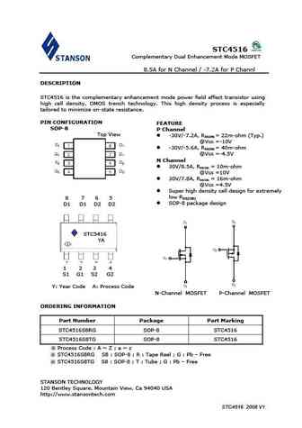
STC4516 Complementary Dual Enhancement Mode MOSFET 8.5A for N Channel / -7.2A for P Channl DESCRIPTION STC4516 is the complementary enhancement mode power field effect transistor using high cell density, DMOS trench technology. This high density process is especially tailored to minimize on-state resistance. PIN CONFIGURATION FEATURE SOP-8 P Channel Top View -30V/-7.2A... See More ⇒
stc4545.pdf
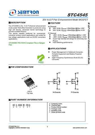
STC4545 30V N & P Pair Enhancement Mode MOSFET DESCRIPTION FEATURE The STC4545 is the N & P-Channel enhancement N-Channel mode power field effect transistor is produced using 30V / 6.8A, RDS(ON) =18m (typ.)@VGS =10V high cell density. advanced trench technology to 30V / 6.0A, RDS(ON) =26m (typ.)@VGS =4.5V provide excellent RDS(ON). This device iswidely prefe... See More ⇒
stc4567.pdf
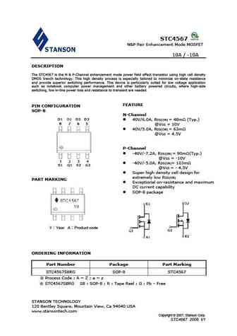
STC4567 N&P Pair Enhancement Mode MOSFET 10A / -10A DESCRIPTION The STC4567 is the N & P-Channel enhancement mode power field effect transistor using high cell density DMOS trench technology. This high density process is especially tailored to minimize on-state resistance and provide superior switching performance. This device is particularly suited for low voltage application su... See More ⇒
stc4539.pdf
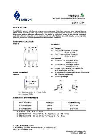
STC4539 N&P Pair Enhancement Mode MOSFET 6.8A / -6.2A DESCRIPTION The STC4539 is the N & P-Channel enhancement mode power field effect transistor using high cell density DMOS trench technology. This high density process is especially tailored to minimize on-state resistance and provide superior switching performance. This device is particularly suited for low voltage application ... See More ⇒
Detailed specifications: IRFU420B, IRFU420PBF, IRFU430APBF, IRFU4510PBF, IRFU4615PBF, IRFU4620PBF, IRFU48ZPBF, IRFU5305PBF, IRF3205, STC4539, STC4545, STC4567, STC4606, STC4614, STC6332, STC6602, STC6614
Keywords - STC4516 MOSFET specs
STC4516 cross reference
STC4516 equivalent finder
STC4516 pdf lookup
STC4516 substitution
STC4516 replacement
Need a MOSFET replacement? Our guide shows you how to find a perfect substitute by comparing key parameters and specs
History: JCS11N90WT | 2SK2267
🌐 : EN ES РУ

LIST
Last Update
MOSFET: AUB034N10 | AUB033N08BG | AUB026N085 | AUA062N08BG | AUA060N08AG | AUA056N08BGL | AUA039N10 | ASW80R290E | ASW65R120EFD | ASW65R110E
Popular searches
tl431 datasheet | 2sd526 | 2n4403 transistor equivalent | 2sc1318 | 2n3055 transistor equivalent | 2sc1740 | c3229 | c2078 transistor