SM2327PSA Specs and Replacement
Type Designator: SM2327PSA
Type of Transistor: MOSFET
Type of Control Channel: P-Channel
Absolute Maximum Ratings
Pd ⓘ
- Maximum Power Dissipation: 1.31 W
|Vds|ⓘ - Maximum Drain-Source Voltage: 30 V
|Vgs|ⓘ - Maximum Gate-Source Voltage: 12 V
|Id| ⓘ - Maximum Drain Current: 4 A
Tj ⓘ - Maximum Junction Temperature: 150 °C
Electrical Characteristics
tr ⓘ - Rise Time: 12 nS
Cossⓘ -
Output Capacitance: 75 pF
RDSonⓘ - Maximum Drain-Source On-State Resistance: 0.056 Ohm
Package: SOT-23-3
- MOSFET ⓘ Cross-Reference Search
SM2327PSA datasheet
..1. Size:256K sino
sm2327psa.pdf 
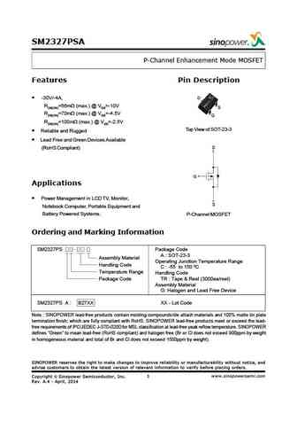
SM2327PSA P-Channel Enhancement Mode MOSFET Features Pin Description -30V/-4A, D RDS(ON)=56m (max.) @ VGS=-10V S RDS(ON)=70m (max.) @ VGS=-4.5V G RDS(ON)=100m (max.) @ VGS=-2.5V Top View of SOT-23-3 Reliable and Rugged Lead Free and Green Devices Available D (RoHS Compliant) G Applications Power Management in LCD TV, Monitor, S Notebook Computer, Portable Equipment and... See More ⇒
9.1. Size:366K taiwansemi
tsm2323 a07.pdf
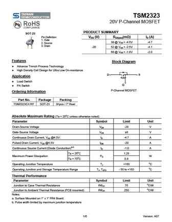
TSM2323 20V P-Channel MOSFET PRODUCT SUMMARY SOT-23 Pin Definition VDS (V) RDS(on)(m ) ID (A) 1. Gate 39 @ VGS = -4.5V -4.7 2. Source 3. Drain -20 52 @ VGS = -2.5V -4.1 68 @ VGS = -1.8V -2.0 Features Block Diagram Advance Trench Process Technology High Density Cell Design for Ultra Low On-resistance Application Load Switch PA Switch P-Chann... See More ⇒
9.2. Size:60K taiwansemi
tsm2328cx.pdf
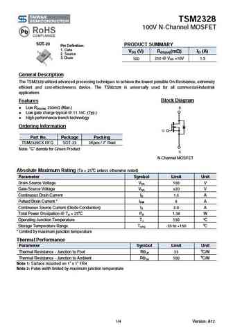
TSM2328 100V N-Channel MOSFET SOT-23 PRODUCT SUMMARY Pin Definition 1. Gate VDS (V) RDS(on)(m ) ID (A) 2. Source 3. Drain 250 @ VGS =10V 1.5 100 General Description The TSM2328 utilized advanced processing techniques to achieve the lowest possible On-Resistance, extremely efficient and cost-effectiveness device. The TSM2328 is universally used for all commercial-in... See More ⇒
9.3. Size:253K taiwansemi
tsm2323cx.pdf
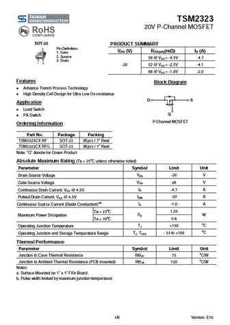
TSM2323 20V P-Channel MOSFET SOT-23 PRODUCT SUMMARY Pin Definition VDS (V) RDS(on)(m ) ID (A) 1. Gate 2. Source 39 @ VGS = -4.5V -4.7 3. Drain -20 52 @ VGS = -2.5V -4.1 68 @ VGS = -1.8V -2.0 Features Block Diagram Advance Trench Process Technology High Density Cell Design for Ultra Low On-resistance Application Load Switch PA Switch P-C... See More ⇒
9.4. Size:164K sino
sm2326nsan.pdf
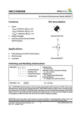
SM2326NSAN N-Channel Enhancement Mode MOSFET Features Pin Description 20V/3A, D RDS(ON)= 70m (max.) @ VGS= 4.5V S RDS(ON)= 90m (max.) @ VGS= 2.5V G RDS(ON)= 110m (max.) @ VGS= 1.8V Top View of SOT-23N Reliable and Rugged Lead Free and Green Devices Available D (RoHS Compliant) G Applications Power Management in DC/AC Inverter Systems S DC-DC Converter ... See More ⇒
9.5. Size:259K sino
sm2329psa.pdf
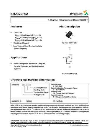
SM2329PSA P-Channel Enhancement Mode MOSFET Features Pin Description -20V/-3.3A, D RDS(ON)= 85m (Max.) @ VGS=-4.5V S RDS(ON)= 120m (Max.) @ VGS=-2.5V G RDS(ON)= 210m (Max.) @ VGS=-1.8V Top View of SOT-23-3 Reliable and Rugged Lead Free and Green Devices Available D (RoHS Compliant) G Applications Power Management in Notebook Computer, Portable Equipment and Battery Powe... See More ⇒
9.6. Size:258K sino
sm2321psa.pdf
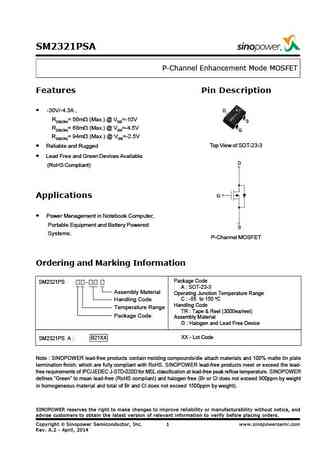
SM2321PSA P-Channel Enhancement Mode MOSFET Features Pin Description -30V/-4.3A , D RDS(ON)= 56m (Max.) @ VGS=-10V S RDS(ON)= 68m (Max.) @ VGS=-4.5V G RDS(ON)= 94m (Max.) @ VGS=-2.5V Top View of SOT-23-3 Reliable and Rugged Lead Free and Green Devices Available D (RoHS Compliant) G Applications Power Management in Notebook Computer, Portable Equipment and Battery Powe... See More ⇒
9.7. Size:254K sino
sm2328nsan.pdf
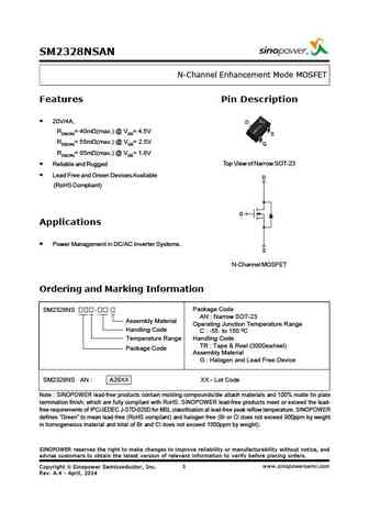
SM2328NSAN N-Channel Enhancement Mode MOSFET Features Pin Description 20V/4A, D RDS(ON)= 40m (max.) @ VGS= 4.5V S RDS(ON)= 55m (max.) @ VGS= 2.5V G RDS(ON)= 85m (max.) @ VGS= 1.8V Top View of Narrow SOT-23 Reliable and Rugged Lead Free and Green Devices Available D (RoHS Compliant) G Applications Power Management in DC/AC Inverter Systems. S N-Channel MOSFET Ordering... See More ⇒
9.8. Size:257K sino
sm2323psa.pdf
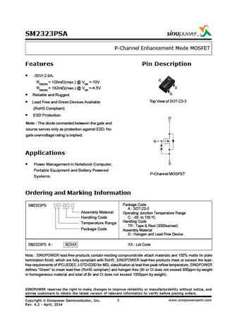
SM2323PSA P-Channel Enhancement Mode MOSFET Features Pin Description -30V/-2.9A, D RDS(ON) = 108m (max.) @ VGS =-10V S RDS(ON) = 182m (max.) @ VGS =-4.5V G Reliable and Rugged Top View of SOT-23-3 Lead Free and Green Devices Available (RoHS Compliant) ESD Protection D Note The diode connected between the gate and source serves only as protection against ESD. No gat... See More ⇒
9.9. Size:257K sino
sm2320nsa.pdf
SM2320NSA N-Channel Enhancement Mode MOSFET Features Pin Description 20V/6.3A , D RDS(ON)=23m (max.) @ VGS=10V RDS(ON)=27m (max.) @ VGS=4.5V S RDS(ON)=40m (max.) @ VGS=2.5V G RDS(ON)=72m (max.) @ VGS=1.8V ESD Protection Top View of SOT-23-3 Reliable and Rugged D Lead Free and Green Devices Available (RoHS Compliant) G Applications Power Management in Notebook Comput... See More ⇒
9.10. Size:832K globaltech semi
gsm2324.pdf
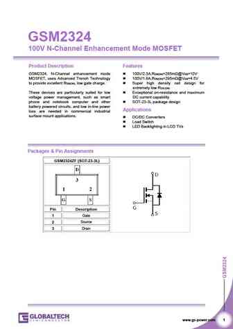
GSM2324 100V N-Channel Enhancement Mode MOSFET Product Description Features GSM2324, N-Channel enhancement mode 100V/2.3A,RDS(ON)=285m @VGS=10V MOSFET, uses Advanced Trench Technology 100V/1.8A,RDS(ON)=295m @VGS=4.5V to provide excellent RDS(ON), low gate charge. Super high density cell design for extremely low RDS (ON) These devices are particularly suited for lo... See More ⇒
9.11. Size:1173K globaltech semi
gsm2323.pdf
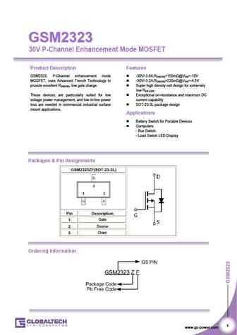
GSM2323 GSM2323 30V P-Channel Enhancement Mode MOSFET Product Description Features GSM2323, P-Channel enhancement mode -30V/-3.6A,RDS(ON)=150m @VGS=-10V MOSFET, uses Advanced Trench Technology to -30V/-3.2A,RDS(ON)=235m @VGS=-4.5V provide excellent RDS(ON), low gate charge. Super high density cell design for extremely low RDS (ON) These devices are particularly suited fo... See More ⇒
9.12. Size:885K globaltech semi
gsm2324a.pdf
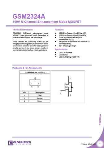
GSM2324A 100V N-Channel Enhancement Mode MOSFET Product Description Features GSM2324A, N-Channel enhancement mode 100V/2.3A,RDS(ON)=310m @VGS=10V MOSFET, uses Advanced Trench Technology to 100V/1.8A,RDS(ON)=320m @VGS=4.5V provide excellent RDS(ON), low gate charge. Super high density cell design for extremely low RDS (ON) These devices are particularly suited for ... See More ⇒
9.13. Size:671K globaltech semi
gsm2323a.pdf
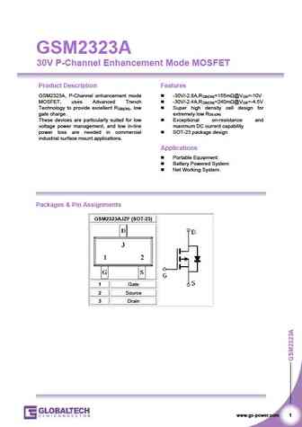
GSM2323A 30V P-Channel Enhancement Mode MOSFET Product Description Features GSM2323A, P-Channel enhancement mode -30V/-2.8A,RDS(ON)=155m @VGS=-10V MOSFET, uses Advanced Trench -30V/-2.4A,RDS(ON)=240m @VGS=-4.5V Technology to provide excellent RDS(ON), low Super high density cell design for gate charge. extremely low RDS (ON) These devices are particularly suited for ... See More ⇒
9.14. Size:870K cn vbsemi
sm2323psa.pdf
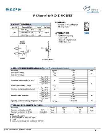
SM2323PSA www.VBsemi.tw P-Channel 30 V (D-S) MOSFET FEATURES PRODUCT SUMMARY TrenchFET Power MOSFET 100 % Rg Tested VDS (V) RDS(on) ( ) Typ. ID (A)a Qg (Typ.) 0.046 at VGS = - 10 V - 5.6 0.049 at VGS = - 6 V - 5 11.4 nC - 30 APPLICATIONS 0.054 at VGS = - 4.5 V -4.5 For Mobile Computing - Load Switch - Notebook Adaptor Switch S TO-236 - DC/DC Converter (SOT-2... See More ⇒
Detailed specifications: SM1A15NSU, SM1A15PSF, SM1C01NSFH, SM1F01NF, SM1F02NSU, SM1F03NSFP, SM1F03NSK, SM1F03NSU, 12N60, SM2328NSAN, SM2558NSUC, SM2602NSC, SM2603PSC, SM2A01NSFP, SM2A02NSU, SM2A06NSFP, MM15N050P
Keywords - SM2327PSA MOSFET specs
SM2327PSA cross reference
SM2327PSA equivalent finder
SM2327PSA pdf lookup
SM2327PSA substitution
SM2327PSA replacement
Need a MOSFET replacement?
Our guide shows you how to find a perfect substitute by comparing key parameters and specs
